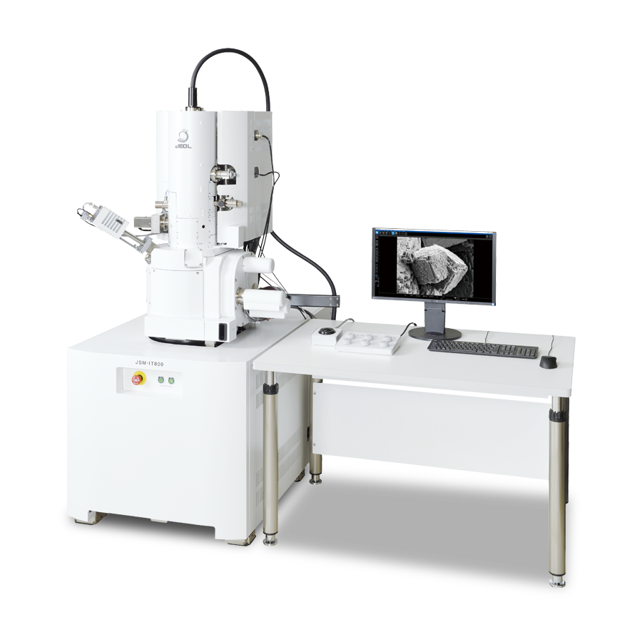
【DISCONTINUED】JSM-IT800
Schottky Field Emission
Scanning Electron Microscope
DISCONTINUED
This product is no longer available.
If you would like to know the latest information about your preferred product or to find out more about alternatives, please click on the link below. We hope you will continue to use our products.
Features
The JSM-IT800 incorporates our "In-lens Schottky Plus field emission electron gun" for high resolution imaging to fast elemental mapping, and an innovative electron optical control system "Neo Engine", as well as a system of seamless GUI "SEM Center" for fast elemental mapping with a fully embedded JEOL energy dispersive X-ray spectrometer (EDS), as a common platform.
The JSM-IT800 allows for the replacement of the objective lens of the SEM as a module, offering different versions to satisfy various users requirements. With the JSM-IT800, five versions are available with different objective lenses: a hybrid lens version (HL), which is a general-purpose FE-SEM; a super hybrid lens version (SHL/SHLs, two versions with different functions), which enables higher resolution observation and analysis; and the newly-developed semi-in-lens version (i/is, two versions with different functions), which is suited for the observation of semiconductor devices.
Furthermore, the JSM-IT800 can also be equipped with a new Scintillator Backscattered Electron Detector (SBED) and a Versatile Backscattered Electron Detector (VBED). The SBED enables the acquisition of images with high responsiveness and produces sharp material contrast even at a low accelerating voltage, while the VBED can help obtain images of 3D, topography and material contrasts. Thus, the JSM-IT800 can help users to obtain information that was not obtainable and to solve problems in measurement.
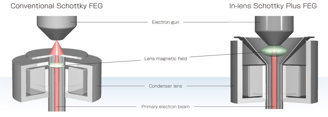
In-Lens Schottky Plus Field Emission Election Gun (FEG)
The integrated In-Lens Schottky Plus and low aberration condenser lens achieves high beam brightness. Ample probe current (100nA@5kV) is available even at low accelerating voltage. This allows the user to perform high resolution observation, high speed elemental mapping, EBSD analysis and Soft X-ray analysis with minimal adjustment of SEM parameters.
Neo Engine (New Electron Optical Engine)
The nex-generation electron optical control system, a masterpiece of JEOL's electron optics technologies is incorporated. Stable observation is possible while adjusting various microscope parameters. Furthermore, the system features enhanced auto-functions for additional ease of use.
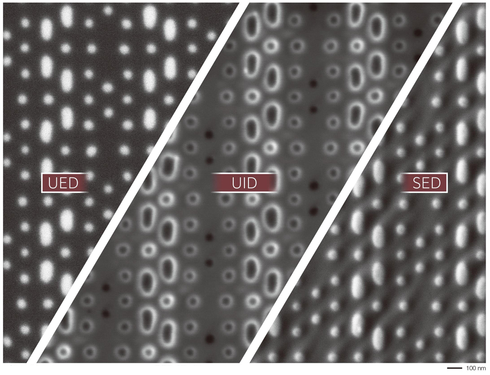
AFS・ACB
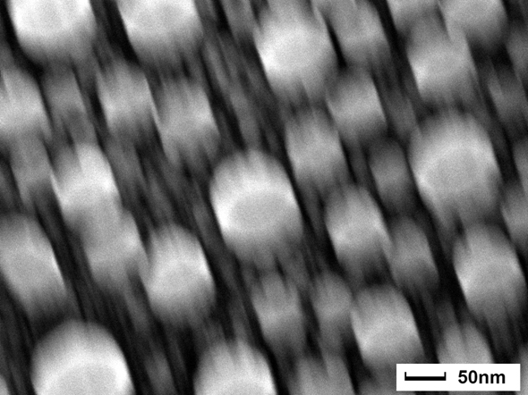
Before auto focus adjustment
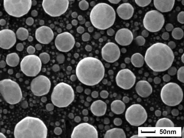
After auto focus adjustment
Specimen: Sn nanoparticles on carbon
Accelerating voltage: 15 kV, WD: 2mm, Observation mode: BD, Detector: UED, Magnification: x200,000
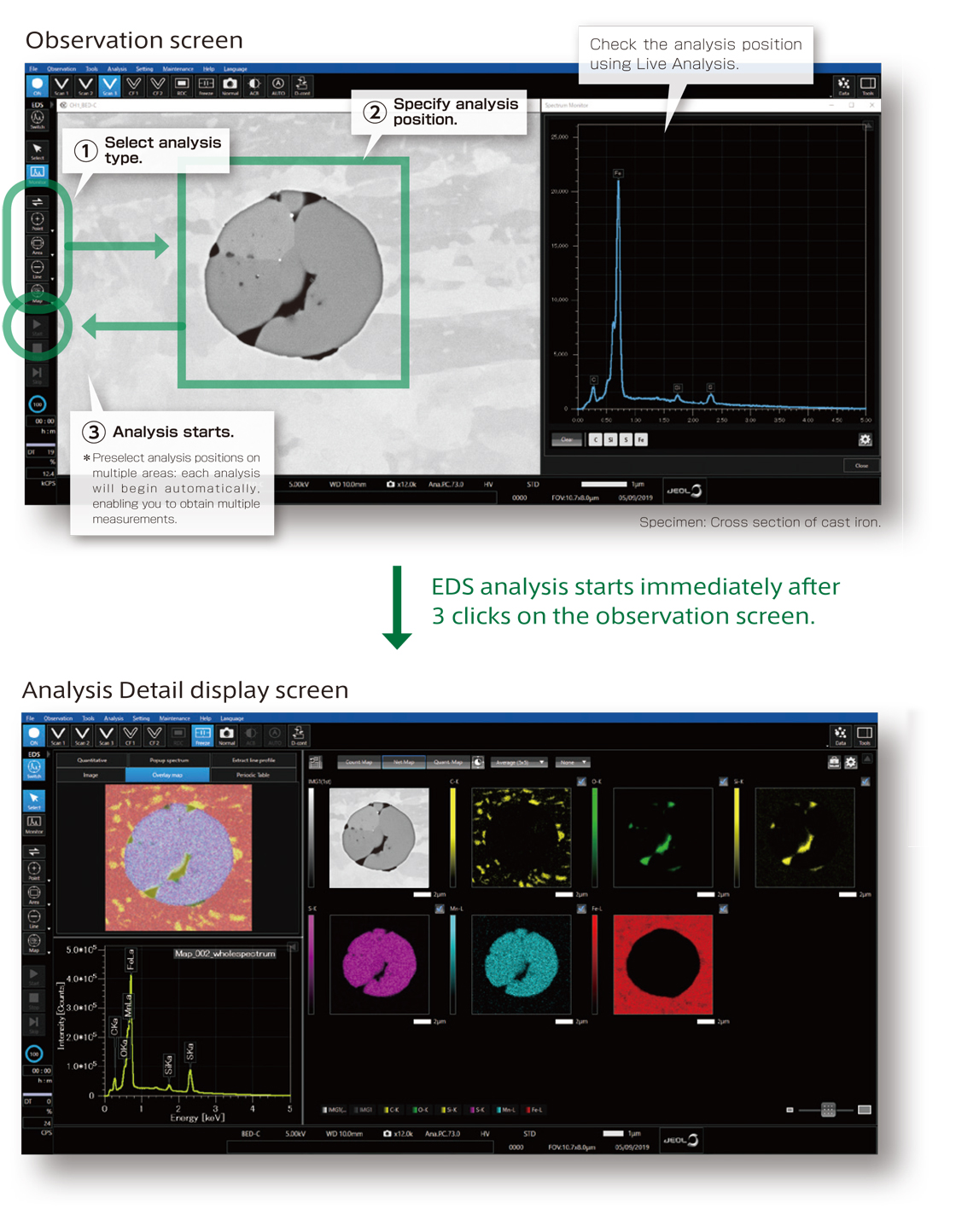
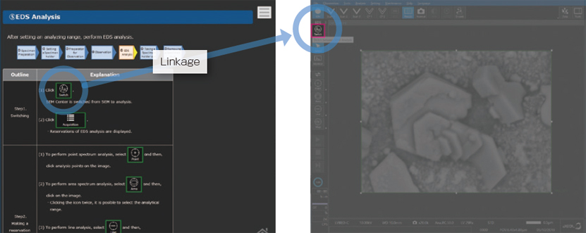
SEM Center・EDS integration
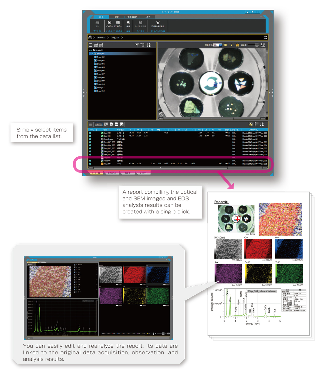
Full integration of microscope GUI "SEM Center" and JEOL EDS has brought about the next generation of SEM utilization. Moreover, the JSM-IT800 incorporates Smile Navi (optional) that can assist a beginner with how to operate an SEM, LIVE-AI (artificial intelligence) filter Live-AI (Live Image Visual Enhancer-AI:LIVE-AI)(optional) providing easy viewing of live image, and SMILE VIEW™ Lab for fast report generation.
SMILE VIEW™ Lab
SMILENAVI *Option
SMILENAVI is an assistant tool designed for beginners to allow smooth basic SEM operations. When the operator clicks on the appropriate button as indicated by the SMILENAVI flowchart, the SEM GUI is linked to the click operation for operator guidance. Since the GUI displays operation steps and button locations, operators will be able to operate the SEM without using SMILENAVI.
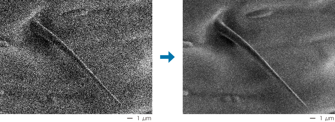
LIVE-AI filter (Live Image Visual Enhancer-AI:LIVE-AI)
Utilizing the AI (artificial intelligence) capability, LIVE-AI filter is incorporated for a higher quality of live images. Unlike image integration processing, this new filter can display a seamless moving live image with no residual image. This unique feature is very effective for quickly searching observation areas, focusing, and stigmator adjustment.
Comparison of live images
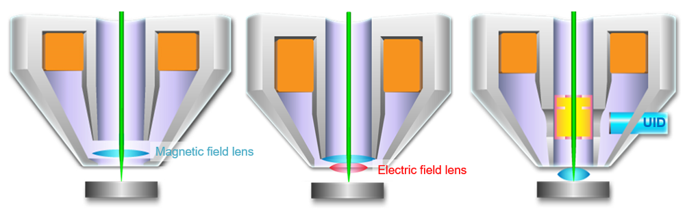
Hybrid Lens version (HL;Hybrid Lens) /
Super Hybrid Lens version (SHL;Super Hybrid Lens) /
Semi-In-Lens version
The JSM-IT800 series offers a choice of objective lenses to suit the user's purpose.
The HL version and SHL version(including SHLs version) are equipped with an electromagnetic/electrostatic field superposed objective lens developed from the versatile out-lens.
The high resolution observation and analysis of a wide variety of specimens from metals to nano materials are possible. It is especially useful for the observation of magnetic materials and analysis such as EBSD measurement.
The i version and is version are equipped with a semi-in lens. They are optimal for high-resolution observation and analysis of tilted and cross-sectional samples, which are necessary for failure analysis of semiconductor devices.
In addition, it is useful for potential contrast observation using an upper in-lens detector (UID).
| Out-lens type | Electromagnetic/electrostatic field superposed objective lens | Semi-In-Lens |
|
High versatility System: JSM-IT700HR |
Versatility and high resolution System: JSM-IT800HL/SHL |
High resolution System: JSM-IT800i/is |
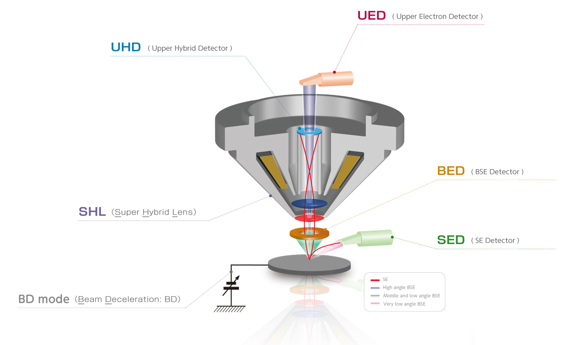
UHD;Upper Hybrid Detector
UHD, a new detector incorporated in SHL version objective lens is highly efficient in detection electrons arising from the specimen, enabling acquisition of images with enhanced S/N ratio.
UHD(Upper Hybrid Detector)
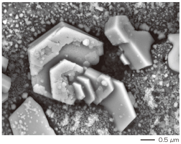
SHL observation example
Specimen: Aluminium Oxide particles
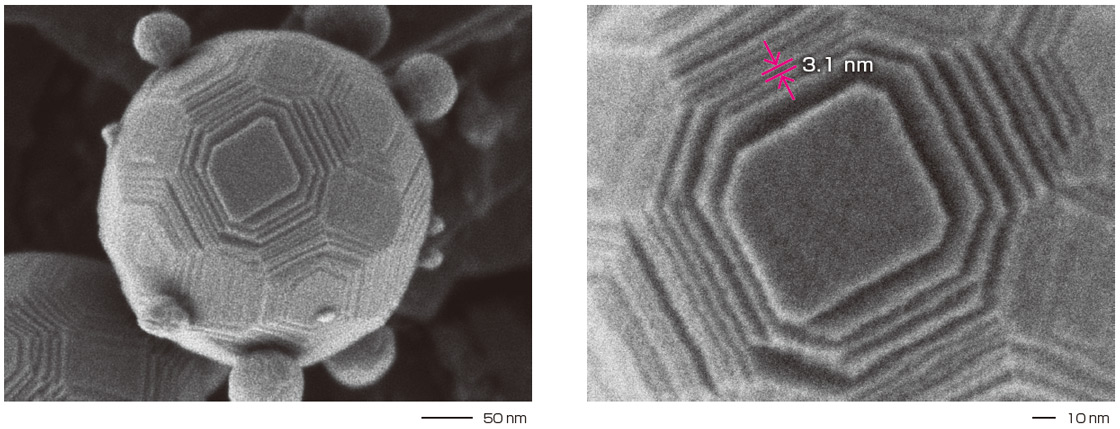
Accelerating voltage: 0.5 kV, Observation mode: BD, Detector: UHD
The amazing step-structure on the surface of particles can be observed. Single nm steps are clearly observed on the particle surface.
※ Acquired by the SHL version.
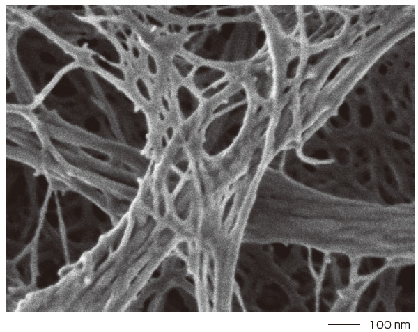
Specimen: Aluminum Boehmite
Accelerating voltage: 0.3 kV, Observation mode: BD, Detector: UHD
The thin nanosheet-structure with less than 10 nm thickness can be clearly observed on the surface of aluminum boehmite.
Acquired by the SHL version.
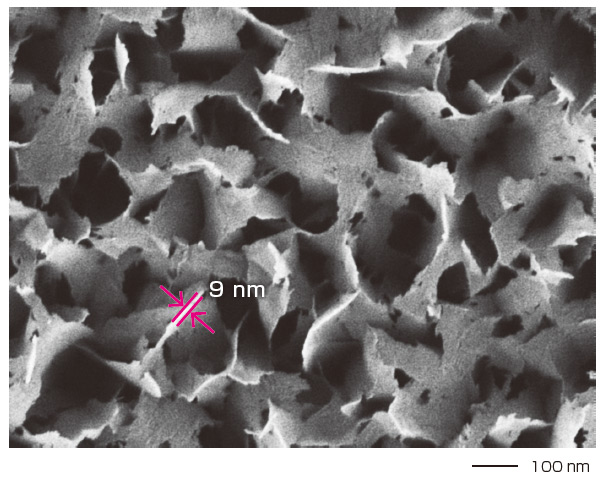
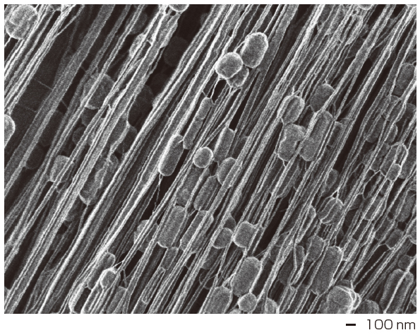
Specimen: Cellulose Nanofiber (CNF)
Accelerating voltage: 0.2 kV, Observation mode: BD, Detector: UHD+UED (signal addition)
Specimen courtesy of Professor Hiroyuki Yano (Research Institute for Sustainable Humanosphere, Kyoto University, Japan)
Although the specimen is an organic fiber, the observation is also feasible through controlling the beam damage on the organic fiber.
Acquired by the SHL version.
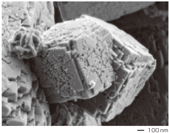
Specimen: Cross section of IC-chip (surface-etching, osmium coating)
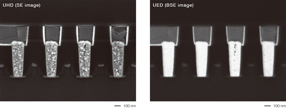
Accelerating voltage: 5.0 kV (without BD mode), Observation mode: SHL, Detector: UHD, UED (BSE mode)
The SE image can be obtained by using the UHD; and the BSE image can be obtained by using the UED.
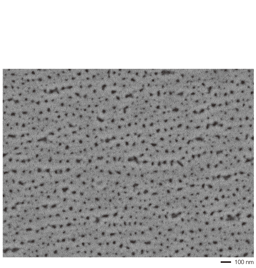
HL observation example
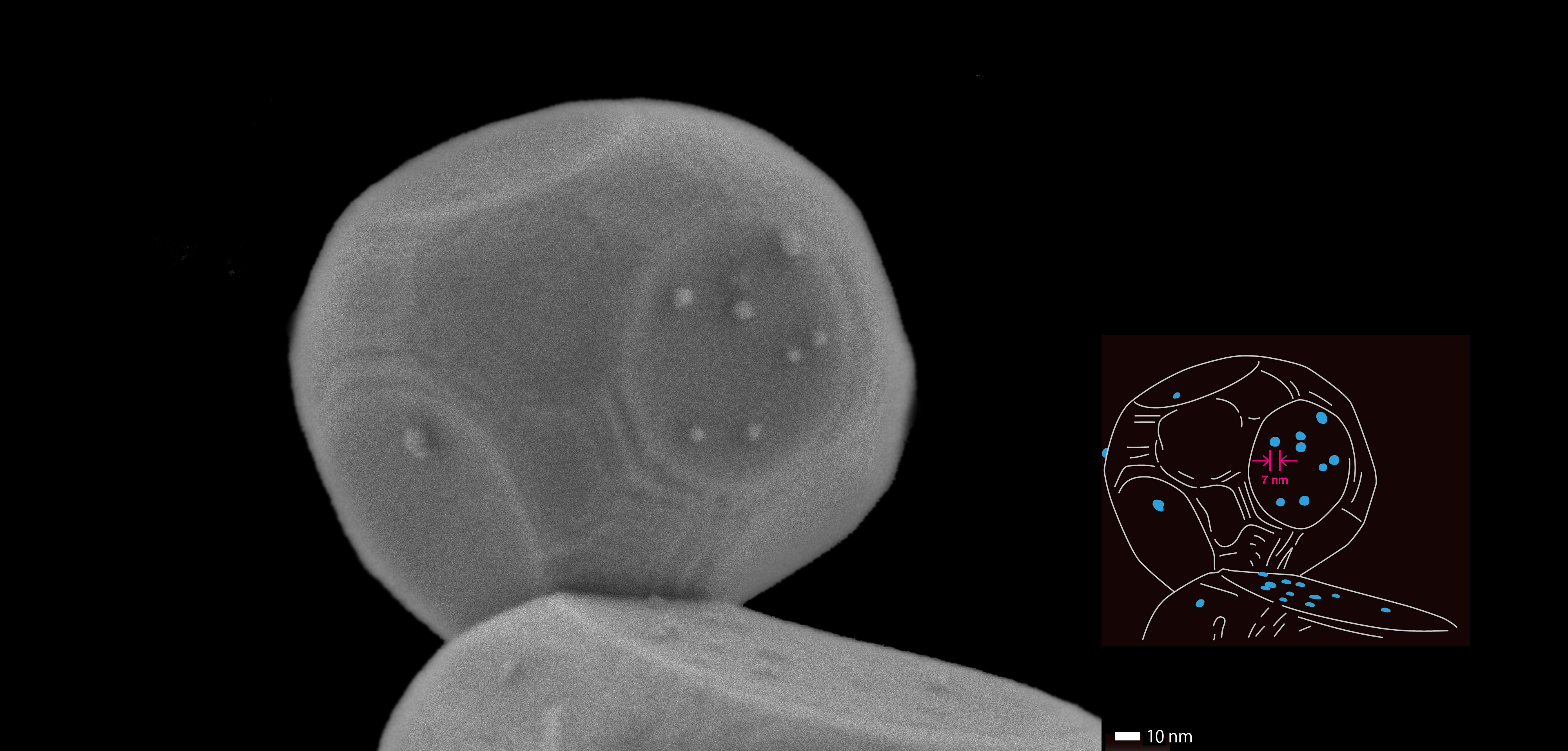
Specimen: Pt nanoparticles on carbon
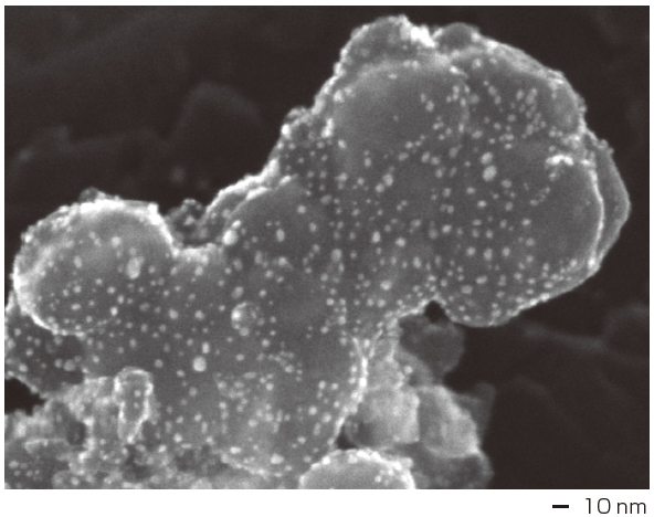
Accelerating voltage: 20 kV, WD: 2 mm, Observation mode: BD, Detector: UED
Specimen: Zeolite
Accelerating voltage: 1 kV, WD: 3 mm, Observation mode: STD, Detector: SED
Specimen: Seal tape
Accelerating voltage: 0.5 kV, WD: 2 mm, Observation mode: BD, Detector: UED
Specimen: Electric lamp lead
Accelerating voltage: 10 kV, WD: 6 mm, Observation mode: LV, Detector: LVBED
i observation example
Secondary electron (SE) image of photocatalyst particles
This image is obtained using the UED detector of the JSM-IT800(i).
Specimen courtesy of Project Professor Kazunari Domen, The University of Tokyo, Japan.
This photocatalyst reveals the quantum efficiency of the water-splitting reaction close to100%. The high resolution SE image clearly shows that the cocatalyst particles with a size less than 10 nm are preferentially deposited on the {100} crystal facets of cubic particles for promoting the hydrogen and oxygen evolution reactions.
Reference
T. Takata et. al., "Photocatalytic water splitting with a quantum efficiency of almost unity," Nature , 581, 411-414, 2020.
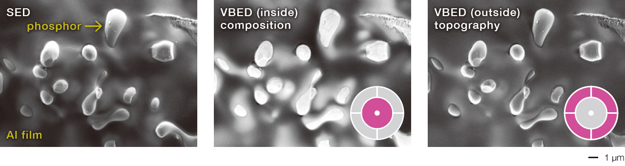
SRAM component Compositional contrast image / Voltage contrast image / Topographic contrast image
Observation conditions: landing voltage 1 kV, WD 8 mm, SIL mode and the signals are obtained by the detectors UED, UID and SED simultaneously
Observation of insulator (uncoated)
Specimen: the surface of Al anodic oxide film
Observation conditions: landing voltage 5 kV, WD 4.5 mm, LV mode (50 Pa), detector LVBED
The nano-pores on the surface can be observed without charging effects when using low vacuum.
In-situ observation of particles dispersed in a liquid Specimen: CeO2 dispersed in water
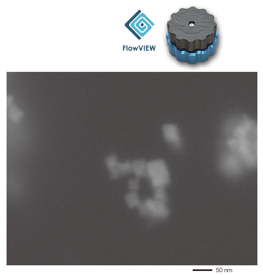
Observation conditions: landing voltage 10 kV, WD 4.5 mm, LV mode (50 Pa), detector LVBED
Enclosing the liquid in the Flow View in-situ holder allows for observation of the particles through the silicon nitride window of holder.
The dispersion of the particles in the liquid also can be observed. (Flow View holder is produced by FlowVIEW Tek)
Reference
N. Asano et. al., "Direct Observation Techniques Using Scanning Electron Microscope for Hydrothermally Synthesized Nanocrystals and Nanoclusters." Nanomaterials , 11, 908, 2021.
New Backscattered Electron Detectors
Scintillator backscattered electron detector (SBED) has excellent sensitivity and is useful in obtaining material contrast image at low acceleration voltage. Versatile backscattered electron detector (VBED) enables acquisition of characteristic images such as 3D and surface topography based on divided detection element shape.
SBED (Scintillator backscattered electron detector)
Use of scintillator for detector has improved detection sensitivity and responsiveness compared to semiconductor element.
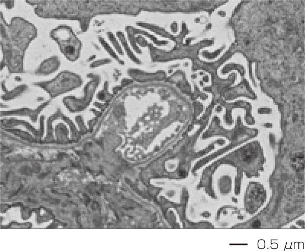
Specimen: ultra-thin section of rat cerebellum (inverse contrast)Accelerating Voltage: 2.0kV
Specimen: toner, Accelerating Voltage: 1.5kV
Specimen: copper plate (observation of transition), Accelerating Voltage:25kV
VBED Images (Versatile Backscattered Electron Detector)
Semiconductor detection element is divided into 5 segments, making it possible to select the signal suitable for the observation purpose.
Angle selection
Specimen: Scintillator, Accelerating Voltage: 3.0kV
Depending on the acquisition angle of backscattered electrons, the composition information is enhanced by the inner segment, while the topography information is enhanced by the outer segments. Moreover, comparing the contrast of fluorescent body beneath the AI deposition film, the different depth related information can be potentially investigated.
3D reconstruction
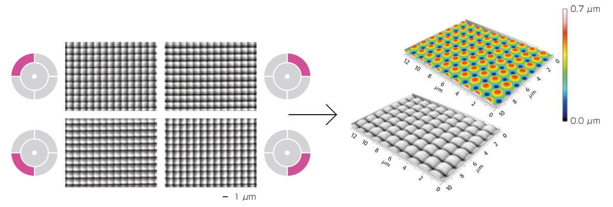
Specimen: On-chip micro lens of CCD element, Accelerating Voltage: 7.0kV
Reconstruction of a 3D image is possible using 2D images obtained from four segments.
Link
News Release
Specifications
| JSM-IT800 (HL) | JSM-IT800 (is) | JSM-IT800 (i) | JSM-IT800 (SHLs) | JSM-IT800 (SHL) | |
|---|---|---|---|---|---|
| Resolution | 0.7nm (20kV) | 0.6nm (15kV) | 0.5nm (15kV) | 0.6nm (15kV) | 0.5nm (15kV) |
| 1.3nm (1kV) | 1.0nm (1kV) | 0.7nm (1kV) | 1.1nm (1kV) | 0.7nm (1kV) | |
| 0.9nm (500V) | |||||
| 3.0nm (15kV, 5nA, WD 10mm) | 3.0nm (15kV, 5nA, WD 8mm) | 3.0nm (15kV, 5nA, WD 8mm) | 3.0nm (15kV, 5nA, WD 10mm) | 3.0nm (5kV, 5nA, WD 10mm) | |
| Magnification | Photo magnification: ×10 to ×2,000,000 (128 × 96 mm) Display magnification: ×27 to ×5,480,000 (1,280 × 960 pixels) |
Photo magnificaton: ×25 to ×2,000,000 (128 × 96 mm) Display magnification: ×69 to ×5,480,000 (1,280 × 960 pixels) |
Photo magnificaton: ×25 to ×2,000,000 (128 × 96 mm) Display magnification: ×69 to ×5,480,000 (1,280 × 960 pixels) |
Photo magnification: ×10 to ×2,000,000 (128 × 96 mm) Display magnification: ×27 to ×5,480,000 (1,280 × 960 pixels) |
Photo magnification: ×10 to ×2,000,000 (128 × 96 mm) Display magnification: ×27 to ×5,480,000 (1,280 × 960 pixels) |
| Landing voltage | 0.01 to 30 kV | ||||
| Probe current | A few pA to 300 nA (30 kV) A few pA to 100 nA (5 kV) |
A few pA to 300 nA (30 kV) A few pA to 100 nA (5 kV) |
A few pA to 500 nA (30 kV) A few pA to 100 nA (5 kV) |
A few pA to 500 nA (30 kV) A few pA to 100 nA (5 kV) |
A few pA to 500 nA (30 kV) A few pA to 100 nA (5 kV) |
| Detector (standard) | Secondary electron detector (SED) Upper electron detector (UED) |
Secondary electron detector (SED) Upper In-lens detector (UID) |
Secondary electron detector (SED) Upper In-lens detector (UID) Upper electron detector (UED) |
Secondary electron detector (SED) Upper hybrid detector (UHD) |
Secondary electron detector (SED) Upper hybrid detector (UHD) |
| Electron gun | In-lens Schottky Plus field emission electron gun | ||||
| Emitter warranty period |
3 years | ||||
| Aperture angle control lens (ACL) | Built-in | Built-in | Built-in | Built-in | Built-in |
| Objective lens | Hybrid Lens | Semi-in-lens | Semi-in-lens | Super hybrid lens | Super hybrid lens |
| Specimen stage | Full eucentric goniometer stage | Full eucentric goniometer stage | Full eucentric goniometer stage | Full eucentric goniometer stage | Full eucentric goniometer stage |
| Stage control | 5-axis motor drive | 5-axis motor drive | 5-axis motor drive | 5-axis motor drive | 5-axis motor drive |
| Specimen size (draw out) |
Type1 (standard) Maximum diameter: 170 mm, Maximum height: 45 mm (WD 5 mm) Stage movement range (X:70mm Y:50mm Z:1 to 41mm Tilt: -5 to 70° Rotation: 360°) Type2 (option) Maximum diameter: 200 mm, Maximum height: 55 mm (WD 5 mm) Stage movement range (X:100mm Y:100mm Z:1 to 50mm Tilt: -5 to 70° Rotation: 360°) Type3 (option) Maximum diameter: 200 mm, Maximum height: 45 mm (WD 5 mm) Stage movement range (X:140mm Y:80mm Z:1 to 41mm Tilt: -5 to 70° Rotation: 360°) |
||||
| Low vacuum mode (option) |
Available | ||||
| Analysis function (option) |
EDS WDS EBSD CL |
EDS WDS EBSD CL |
EDS WDS EBSD CL |
EDS WDS EBSD CL |
EDS WDS EBSD CL |
| Main applications(example) | Magnetic material Wide area EBSD |
Semiconductor device analysis | Magnetic material, EBSD, Biological specimen (Array tomography, CLEM) |
||
Specimen Exchange System
Optical image acquisition supports both specimen exchange systems
Draw-out system suitable for large-specimen exchange
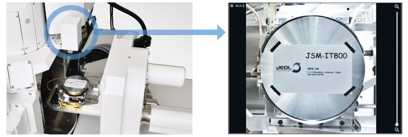
With draw-out system
Max. specimen size: 170 mm diameter
Vacuum evacuation: 3 to 5 minutes
Optical image area: 120 mm × 120 mm
Specimen exchange chamber enabling fast and clean specimen loading/unloading
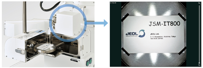
With pre-evacuation chamber
Max. specimen size: 100 mm diameter
Vacuum evacuation: 60 seconds or less
Optical image area: 70 mm × 70 mm
Evacuation and venting times change depending on specimen or installation environments.
The optional stage navigation system (SNS) is required for use of optical images.
The specimen exchange chamber is optional.
Details of DrySD™ detectors
| Detection area | 60 mm2 |
|---|---|
| Energy resolution | 133 eV or less |
| Detectable elements | Be to U |
| Data management function & report creation | SMILE VIEW™ Lab |
Principal Options
Upper electron detector (UED) *SHL, SHLs, is
Upper secondary electron detector (USD) *HL
Upper electron detector (UED) *is
Upper electron converter (UEC) *is
Backscattered electron detector (BED)
Scintillator backscattered electron detector (SBED)
Versatile backscattered electron detector (VBED) *HL, SHL, SHLs
Transmission electron detector (TED)
Low vacuum (included Low vacuum backscattered electron detector (LVBED))
Low vacuum secondary electron detector (LVSED)
Electron backscatter diffraction system (EBSD)
Wavelength dispersive X-ray spectrometer (WDS)
Soft X-ray emission spectrometer (SXES) *HL, SHL, SHLs
Probe current detector
Specimen exchange chamber
Stage navigation system
Chamber camera
Operation table
Operation panel
Track ball
SMILENAVI
Montage
LIVE map
LIVE AI filter
SMILE VIEW™ Map
Catalogue Download
JSM-IT800 Schottky Field Emission Scanning Electron Microscope
Application
Application JSM-IT800
Related Products
Related Products
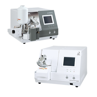
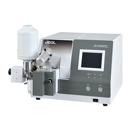
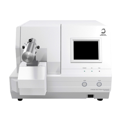
IB-19520CCP CROSS SECTION POLISHER™
Thermal damage can be reduced by cooling the specimen with liquid nitrogen during processing.
Designed to suppress the consumption of liquid nitrogen, allowing long cooling periods.
Rapid cooling of the specimen while immersed in liquid nitrogen. Return to room temperature. Designed to allow parts to be detached.
Incorporates a mechanism to allow the process from polishing to observation to be performed without exposing the sample to the air.
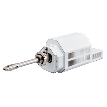
IB-19530CP CROSS SECTION POLISHER™
The IB-19530CP features an innovatively designed, multi-purpose stage to fulfill increasingly diversified market needs and realize multi-functionality by different kinds of functional holders. The multi-purpose stage combined with specialized functional holders allows the user to perform various functions such as planar surface milling and polishing, sputter coating as well as more traditional cross-section ion milling.
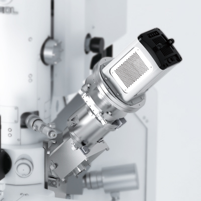
Gather-X JED Series Dry SD™ Windowless EDS
Explore Science with the JSM-IT800/Windowless EDS Analysis
Stress-free EDS analysis from light to heavy elements!Driven by carbon neutrality, material development is becoming more important.
For example, in battery materials, a wide range of analysis is required from light elements such as Li to transition metals including Ni, Co, and Mn.
The needs for efficient and highly sensitive analysis are increasing in the analysis of semiconductor materials and nanoparticles of catalysts.
The newly developed Dry SD™ Gather-X is a Windowless type EDS that is installable to JSM-IT800*. High sensitivity X-ray analysis is possible in all energy bands including low energy characteristic X-rays such as Li-K (54eV). In addition, the safety function interlocked with the JSM-IT800 and the SEM/EDS integration software can provide safe and comfortable operability just to anyone.
*Installable to JSM-IT800<HL>/<SHL/SHLs>.
Soft X-ray Emission Spectrometer(SXES)
The Soft X-Ray Emission Spectrometer (SXES) is an ultra-high resolution spectrometer consisting of a newly-developed diffraction grating and a high-sensitivity X-ray CCD camera.
In the same way as EDS, parallel detection is possible, and 0.3 eV (Fermi-edge, Al-L standard) ultra-high energy resolution analysis can be performed, surpassing the energy resolution of WDS.
More Info
Are you a medical professional or personnel engaged in medical care?
No
Please be reminded that these pages are not intended to provide the general public with information about the products.