


ACE eye™
High Throughput Analytical Electron Microscope
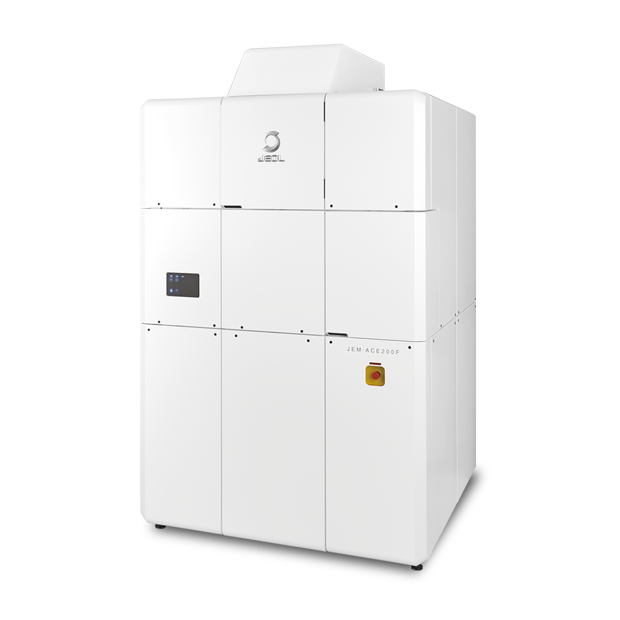
From "operator dependent" to "operator-free measurement"
ACE eye™ is a semiconductor-dedicated TEM that delivers fully automated, end-to-end operation—from TEM/STEM imaging to EDS analysis—through a predefined, recipe-based workflow. By standardizing measurement conditions, it ensures outstanding reproducibility while offering flexible operation modes, ranging from semi-automated to fully automated workflows.
Equipped with AI-driven automatic aberration correction (ASCOR, as a standard) and advanced automation algorithms, ACE eye™ continuously maintains optimal measurement conditions, enabling highly precise, operator-independent results.
In addition, by leveraging proven hardware technologies and a design optimized for long-term stable operation, ACE eye™ delivers the usability and high reliability required for semiconductor analysis.
Features
Automation
By converting measurement conditions and procedures into standardized recipes, ACE eye™ enables fully automated, end-to-end operation—from TEM/STEM imaging to EDS analysis—within a single workflow, ensuring stable, operator-independent results.
The system supports a flexible range of automation levels, from semi-automated to fully automated workflows, allowing users to select the optimal configuration based on their measurement objectives and operational requirements.
ACE eye™ is equipped with ASCOR (by CEOS) as a standard, enabling AI-driven automatic aberration correction. Combined with advanced automation algorithms, it continuously optimizes measurement conditions and maintains peak performance at all times.
Key parameters—including focus adjustment, astigmatism correction, specimen height alignment, beam centering, and crystal orientation alignment—are automatically controlled to ensure consistent and reliable measurements.
The combination of a large-capacity liquid nitrogen tank (with a coolant holding time of approximately five days), the optional Automation Center automated measurement software, and the optional MSP (MultiSPECPORTER) enables unattended, long-duration continuous operation, improving measurement efficiency and maximizing system utilization.
Stability
A robust system design incorporating a wide-gap pole piece and ASCOR (by CEOS) ensures the stable integration of high-resolution imaging and high-sensitivity EDS analysis, providing an optimal observation environment for advanced semiconductor material characterization.
High magnification reproducibility of ±0.5% is achieved for both TEM and STEM, enabling stable positioning and reliable data acquisition even during a long-duration or fully automated measurements.
Continuous monitoring of system status and external environmental factors—including magnetic fields, vibration, room temperature, and cooling water temperature—via LogChecker (optional) provides full visibility into the measurement environment and ensures a consistent, stable operation.
The column enclosure minimizes the impact of external disturbances, further enhancing reproducibility and reliability in automated measurements and high-magnification observations.
Operability
The intuitive user interface, “TEM Center”, enables a seamless execution from observation to measurement using a mouse, ensuring smooth workflows independent of user experience.
“Automation Center”, features two dedicated modes—Operator and Administrator—facilitating an efficient configuration and operational management based on user roles.
Seamless integration with Gatan cameras supports smooth workflows from image acquisition to data storage, enabling high-productivity observation while delivering highly reliable data.
A newly developed holder enables one-touch loading and removal of specimen grids, simplifying operation, reducing routine workload, and shortening preparation time.
FIB Linkage
Optional dual-axis tilt cartridges and dedicated TEM holders enable seamless integration between TEM and FIB workflows.
The cartridge can be attached to the dedicated holder in a single action, eliminating the need for direct handling of TEM grids after specimen preparation. This reduces operator workload while minimizing the risk of specimen damage and contamination.
Specifications
| TEM resolution(at 200 kV) |
|
||||||
|---|---|---|---|---|---|---|---|
| STEM resolution (at 200 kV) |
|
||||||
| Electron gun | Cold field emission gun (CFEG) | ||||||
| Accelerating voltage | 60 kV to 200 kV (80, 200 kV : standard, other voltages : optional) |
||||||
| Aberration corrector | STEM:ASCOR (standard) | ||||||
| Specimen movements | X,Y ±1.0 mm Z ±0.4 mm | ||||||
| Specimen tilt angle |
|
||||||
| Options | JEOL 160 mm2 SDD(Dual), Automation Center, MultiSPECPORTER, Tomography, EELS |
Gallery
LAADF-STEM image
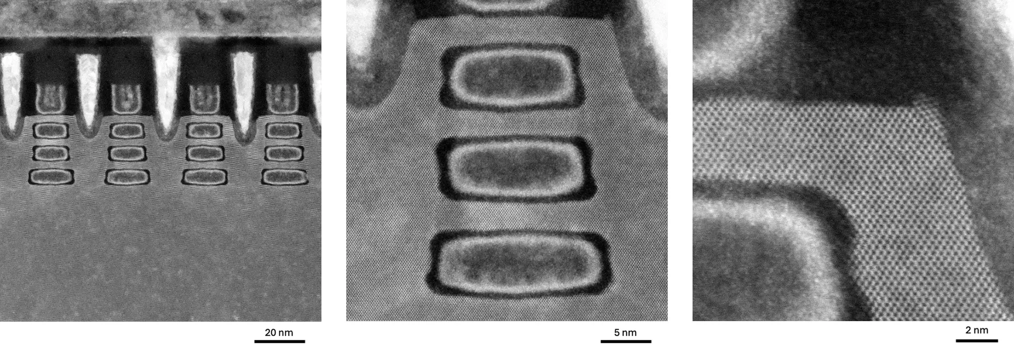
Specimen : Semiconductor device (GAA)
Accelerating voltage : 200 kV
HAADF-STEM image (CD Measurement )
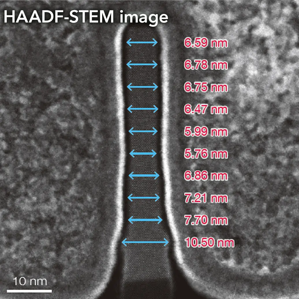
Specimen : Semiconductor device (FinFET)
Accelerating voltage : 200 kV
EDS maps (Net count map)
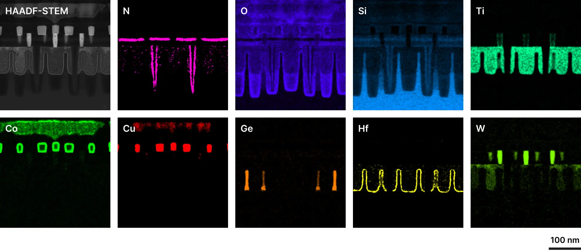
Specimen : Semiconductor device (FinFET)
Accelerating voltage : 200 kV
Related Products
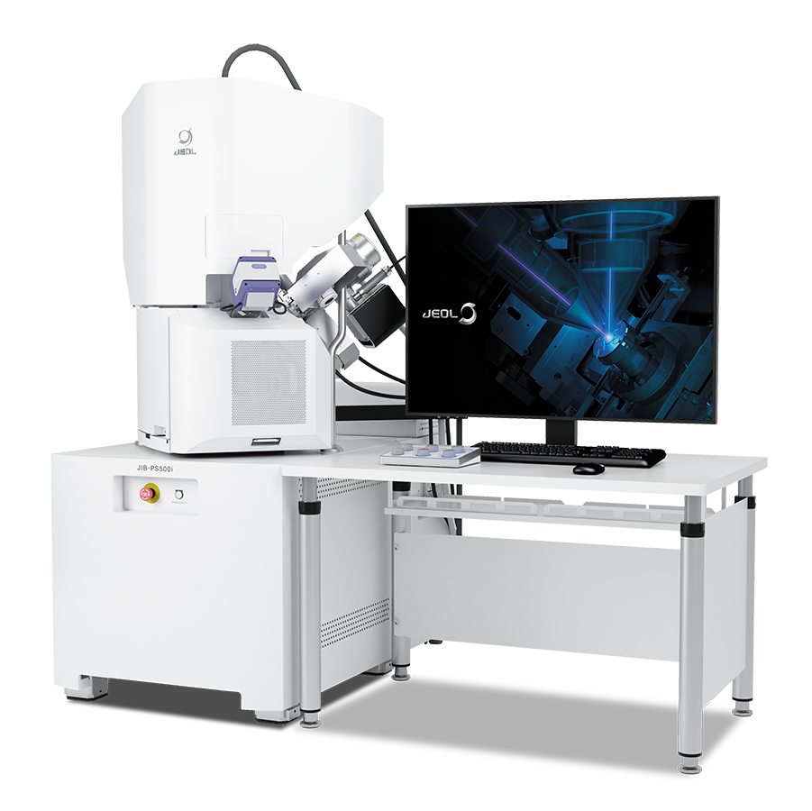
JIB-PS500i FIB-SEM system
The JIB-PS500i provides three solutions to assist TEM specimen preparation. High throughput workflow is assured from specimen prepartion to TEM observation.
More Info


Are you a medical professional or personnel engaged in medical care?
No
Please be reminded that these pages are not intended to provide the general public with information about the products.