JAMP-9510F
Field Emission Auger Microprobe
 Powered by Bioz
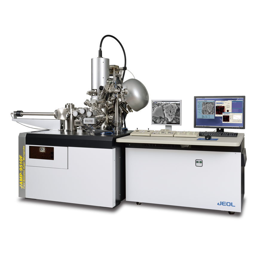
It is a high specification Auger electron spectrometer with a hemispherical analyzer to provide high throughput analysis of the chemical bonding state at nano to micro areas, and a field emission electron gun also used for EPMA, because it can deliver a large, stable electric current The highly precise eucentric specimen stage makes it possible to perform the previously-impossible analysis of insulators. This in combination with the floating type ion gun offers the versatility to handle any specimen, such as metals and insulation materials, to obtain composition information to and chemical information.
Features
Spectrum imaging
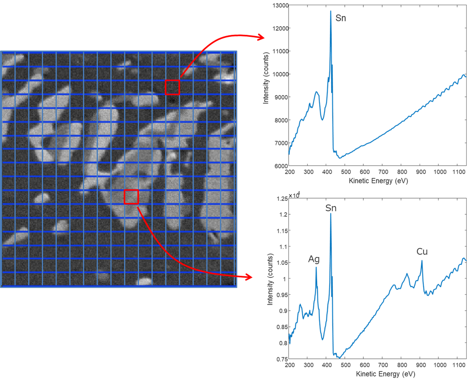
Each pixel contains spectrum
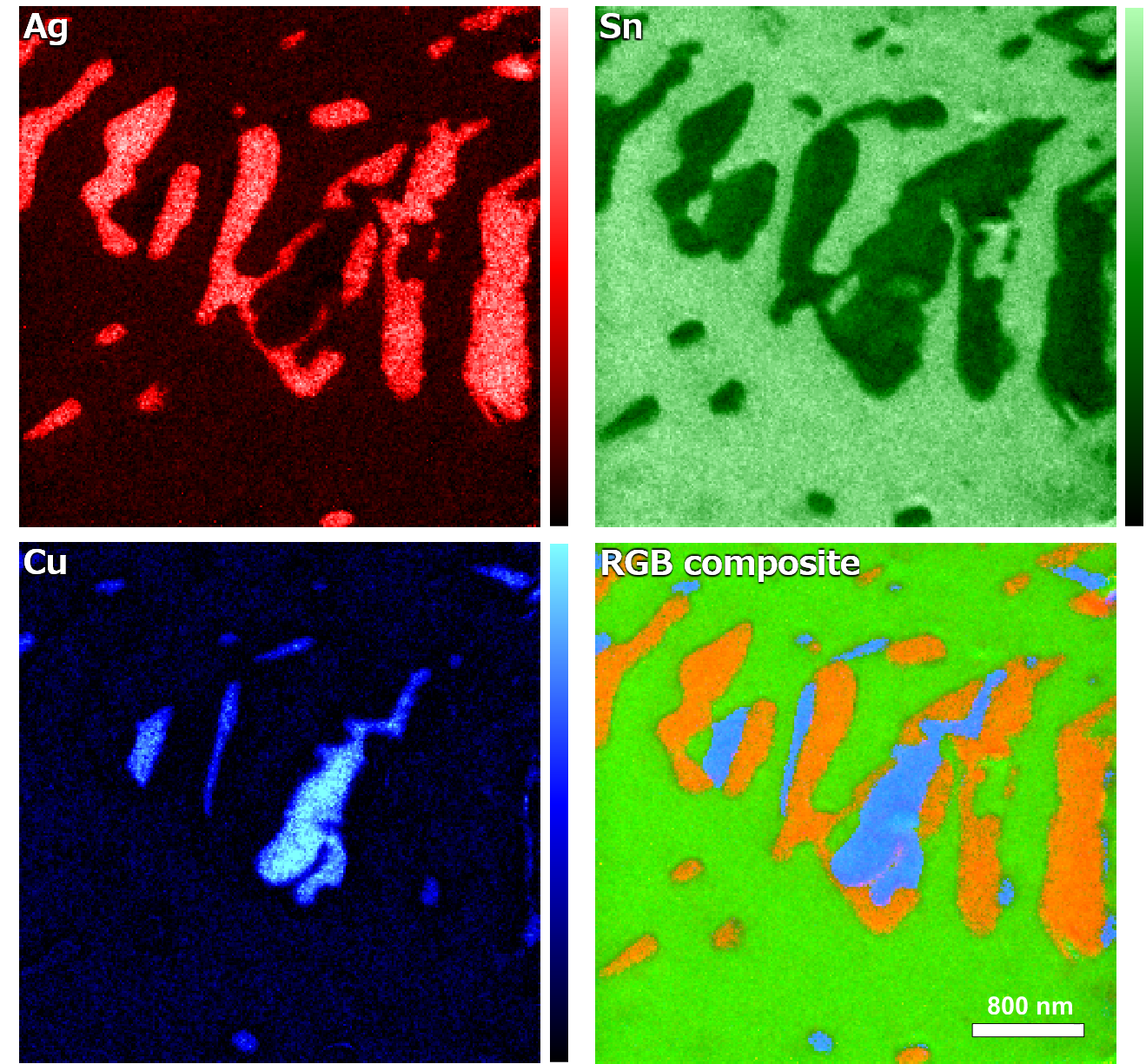
Elemental distributions extracted
from a spectrum image data cube
A newly-developed spectrum imaging method enables to capture electron spectra for each pixel in the image. Spectra in the selected areas in the image and elemental distributions can be extracted after the acquisition of the data, like EDS mapping. The spectrum imaging method prevents missing any elements by acquiring data in a wide energy range, which is totally different from conventional Auger mapping, where, elements to be mapped should be specified in advance. The measuring energy range and energy resolution are selectable as well as usual wide spectrum acquisition. Spectrum imaging can be applied not only to elemental analysis but also to reflection electron energy loss spectroscopy (REELS) analysis.
Standard spectra database & peak deconvolution software
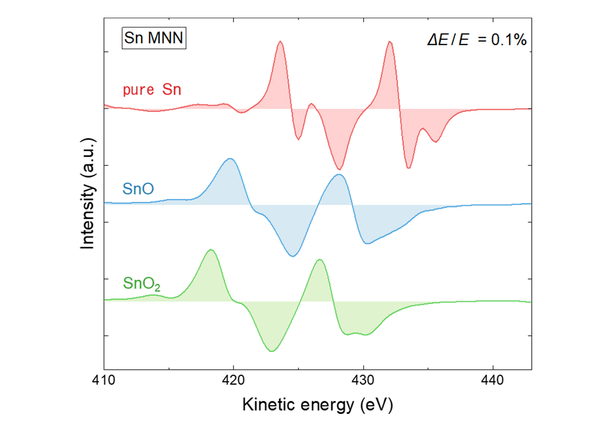
Standard spectra of pure Sn, SnO and SnO2
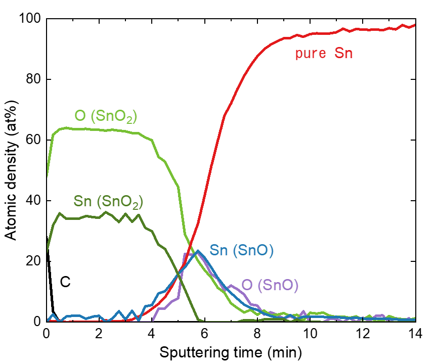
Chemical-state resolved depth profile of the solder surface
Standard spectra database of over 500 spectra for 140 materials is provided. Our peak deconvolution software easily separates overlapped Auger peaks and also enables a complicated chemical state analysis with one click.
Research Publications Using JAMP-9510F
Specifications
| Electron illumination system | |
|---|---|
| SEI resolution | 3nm(at 25kV, 10pA) |
| Probe diameter for Auger analysis | 8nm(at 25kV, 1nA) |
| Electron gun | Schottky field emission gun |
| Accelerating voltage | 0.5 to 30kV |
| Probe current | 10-11 to 2×10⁻⁷A |
| Magnification | x 25 to 500,000 |
| Auger analysis system | |
| Analyzer | Electrostatic hemispherical analyzer (HSA) |
| Energy resolution(ΔE/E) | 0.05 to 0.6% |
| Sensitivity | 840,000 cps/7 ch or more
(at 10 kV 10 nA Cu-LMN, 0.6% resolution, 60tilt) |
Specifications subject to change without notice.
Expandability
Additional ports to accommodate the following attachments are pro-vided, supporting a variety of analyses.
Additional ports to accommodate the following attachments are pro-vided, supporting a variety of analyses
Specimen Parking Unit
Specimen Cooling and Fracturing Device
Backscattered Electron Detector
Energy Dispersive X-ray Spectrometer (EDS)
Transfer Vessel
Catalogue Download
JAMP-9510F Field Emission Auger Microprobe
Application
Semiconductor devices
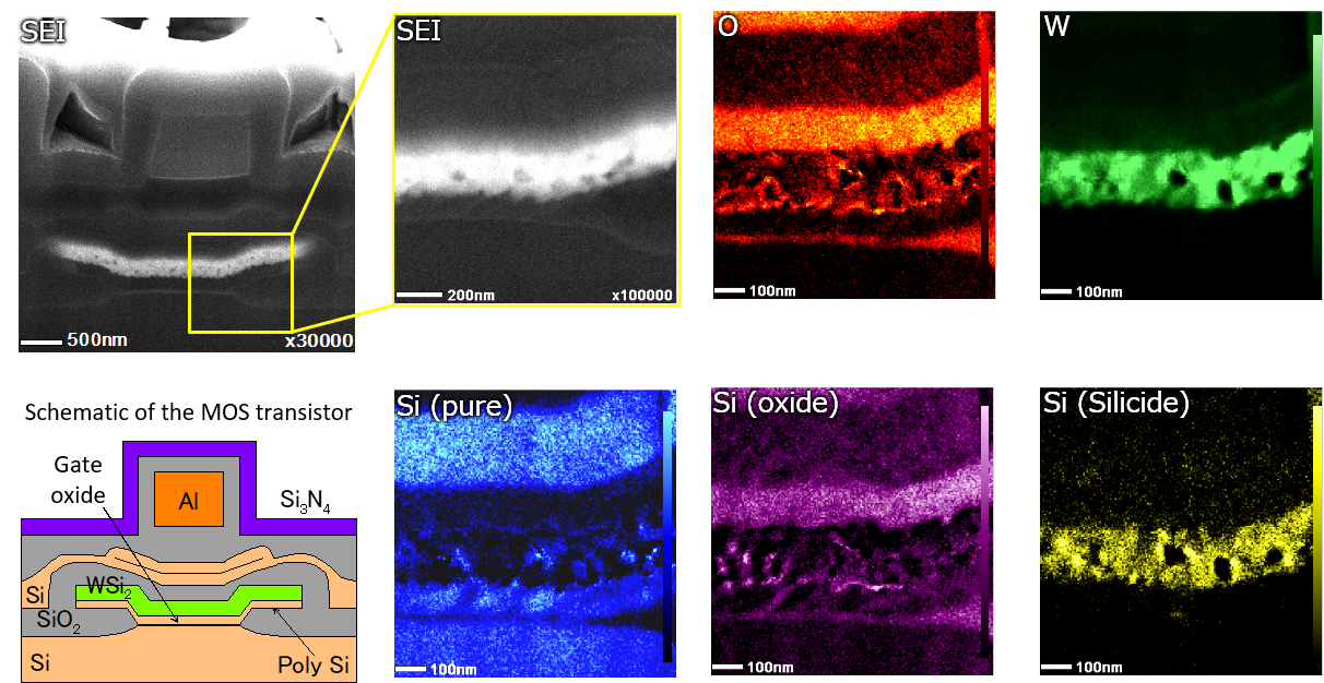
Elemental distributions and chemical state mapping of silicon of a cross-section of a semiconductor device,
acquired by spectrum imaging.
Compared with X-ray emission spectroscopy like SEM-EDS and EPMA, spatial resolution of AES analysis is very high. AES analysis can be applied to elemental analysis in the high magnification field of view. Chemical state mapping is also possible by utilizing differences of Auger peak shapes by chemical state of the sample.
Lithium-ion battery (LIB) materials
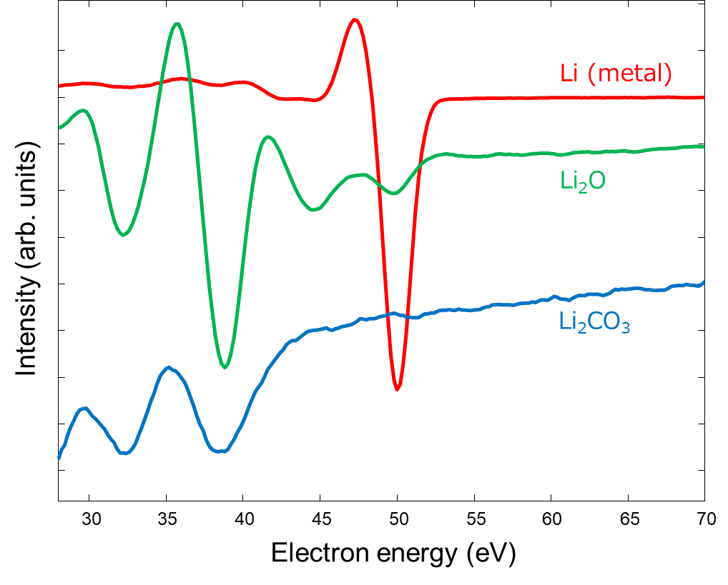
Standard spectra of Li KVV in the differential form
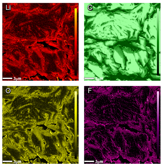
Cross-section elemental mapping for a LIB anode material
Lithium detection sensitivity of AES is high and often used for analysis of lithium-ion battery materials. AES detects lithium peaks from lithium oxides and lithium carbonate with good sensitivity because electrons at the adjacent atoms get involved in the auger process. Lithium mapping can be performed easily with spectrum imaging.
REELS analysis
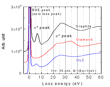
Loss spectra of carbon materials
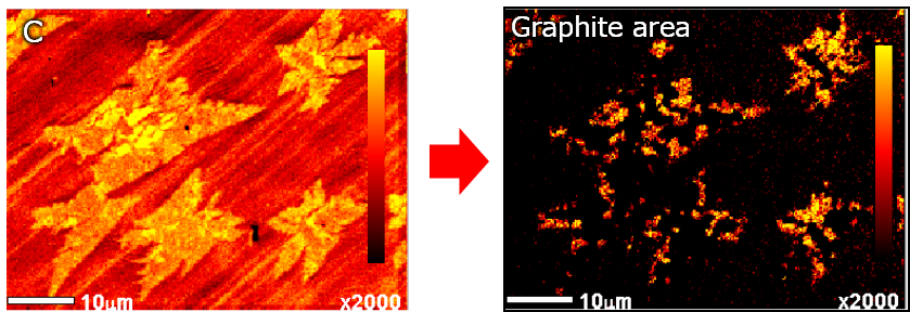
Carbon distribution obtained by AES analysis (left) and graphite distribution by REELS analysis (right) for a graphene sample on a copper plate
Reflection electron energy loss spectroscopy (REELS) is also an important application of Auger microprobe. REELS is applied to analysis of carbon materials and also to evaluation of the bandgap size of wide-bandgap semiconductors and insulators.
Other applications for JAMP-9510F
More Info
Are you a medical professional or personnel engaged in medical care?
No
Please be reminded that these pages are not intended to provide the general public with information about the products.