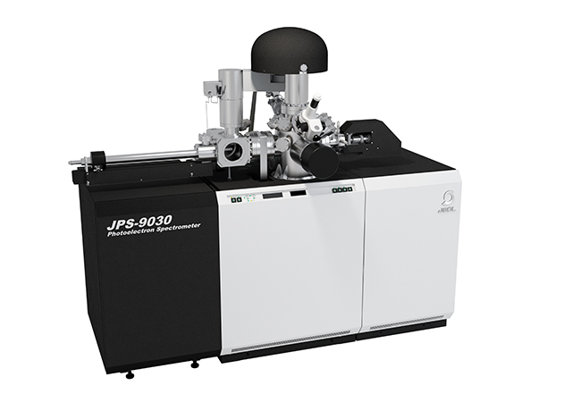
JPS-9030
Photoelectron Spectrometer
 Powered by Bioz
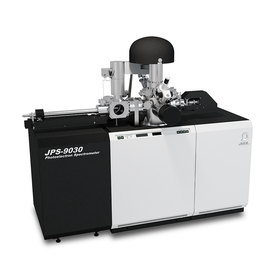
By adopting the newly-designed user interface that allows for operation in Japanese environment, ”Easy, Immediate operation just for Anyone” has been realized. In addition, equipping a Kaufman-type etching ion source and a twin anode as standard, the JPS-9030 has a wide range of expandability such as a high temperature heating system and a gas cluster ion source.
Features
①Wide area analysis that can be measured in a short time
The JPS-9030 is an XPS that can analyze a wide area of specimens, such as analysis area of millimeter order, and is optimal for average value analysis. It enables the acquisition of specimen information regardless of segregation and local contamination of a specimen. It is suitable for elemental analysis chemical bonding state analysis of specimens of powder, thin film, and plate.
〇Example of utilization of wide area analysis - Elemental analysis of LIB cathode material
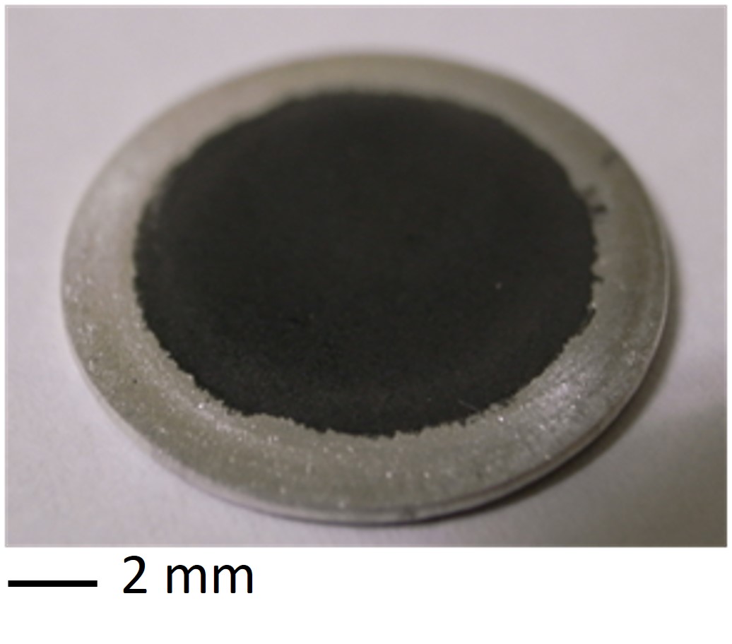
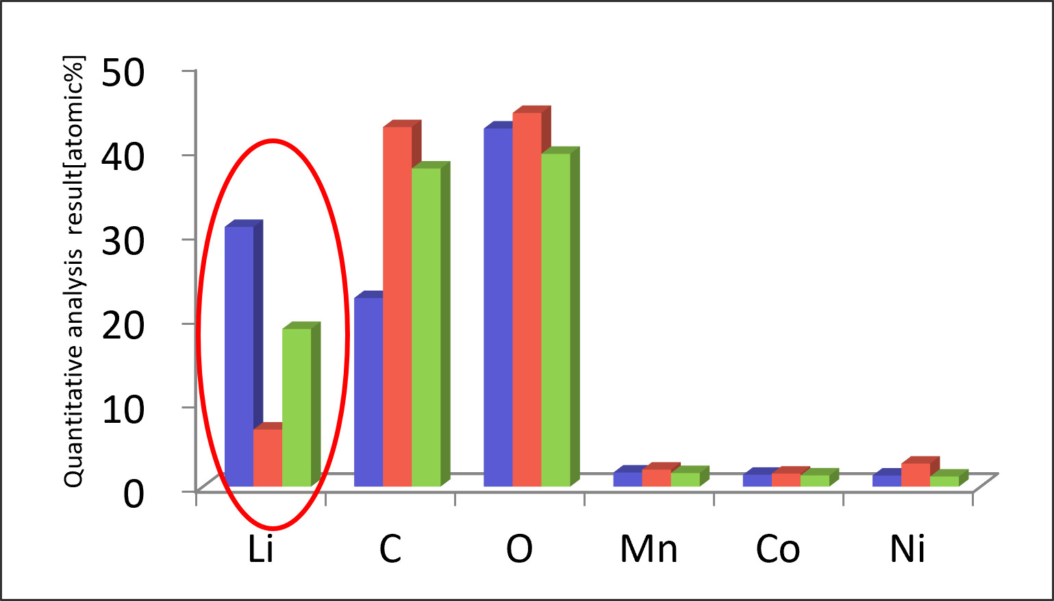
At first glance, LIB cathode materials appear to be uniform. However, if the analysis range is narrow, the results of elemental analysis may vary. It is possible to obtain the average information without the influence of local contamination by widening the analysis range.
Measurements were taken at three locations to narrow down the analysis range.
⇒There was a large variation in results.
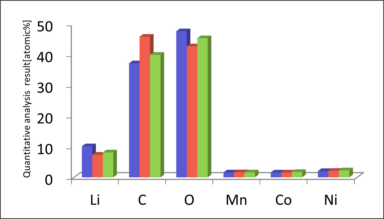
Measurements were taken at three locations to narrow down the analysis range.
⇒There was a small variation in results.
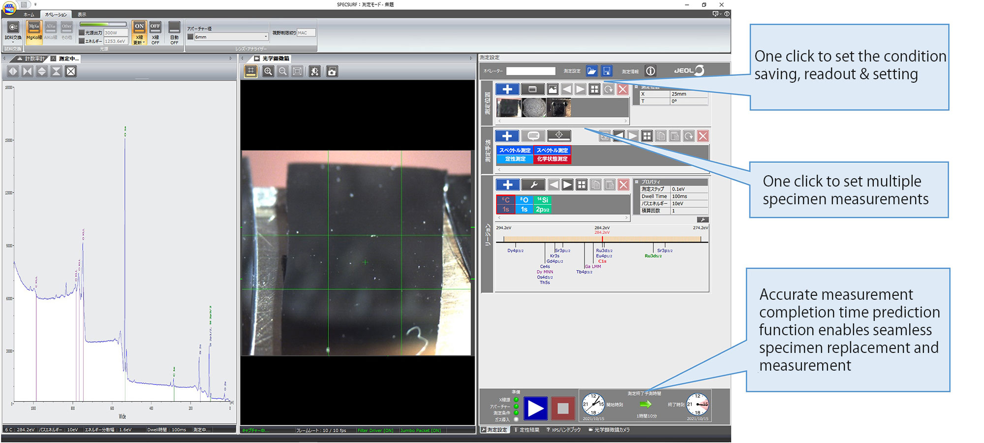
②Software SPECSURF enabling easy operations
The newly developed software SPECSURF Ver. 2.0 for Japanese language, provides
a user-friendly operation environment with the mouse only, by combining Ribbon-style GUI and a tab window system.
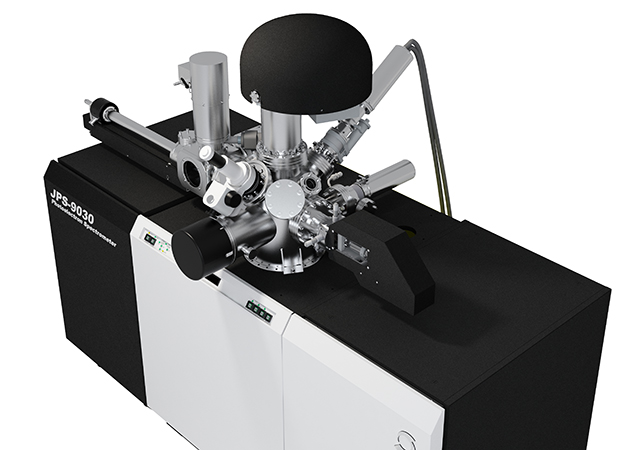
③Instrument configuration enabling measurement of a wide range of materials – Mg/Al twin anode X-ray source-
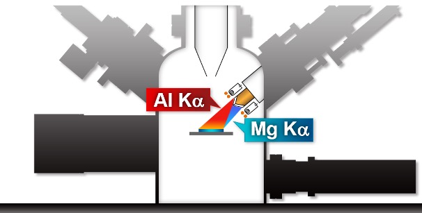
With the JPS-9030, a monochromatic X-ray source and Mg/Al twin anode X-ray source can be used. The Mg/Al twin anode x-ray source can switch the x-rays to irradiate a specimen between Mg K ray and Al K ray, which makes it possible to analyze a specimen that contains many elements and with which the photoelectron peak and Auger peak overlaps.
-One click to set the condition saving, readout & setting
-One click to set multiple specimen measurement
-Accurate measurement completion time prediction function enables seamless
specimen replacement and measurement
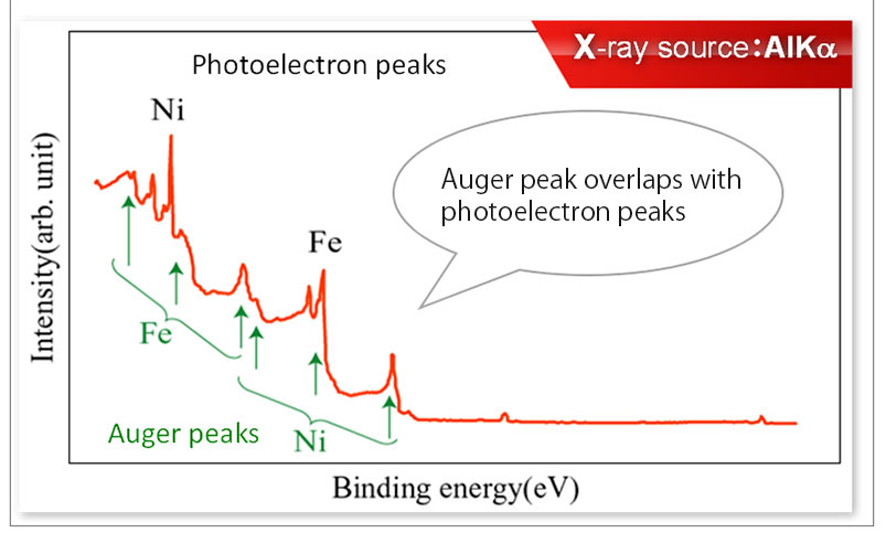
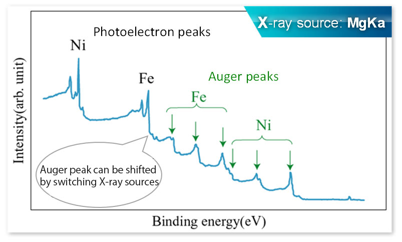
〇Example of utilization of Mg/Al twin anode X-ray source-Analysis of a specimen containing Fe, Ni
On the XPS spectrum, one of the examples where the photoelectron peak and Auger peak overlaps is a specimen containing several elements of transition metal. The following is the measurement example of a specimen containing Fe and Ni. It shows that the peak overlapping observed with an Al X-ray source, can be avoided with a Mg X-ray source.
Measurement by Al X-ray source
⇒Peak overlap
Measurement by Mg X-ray source
⇒Avoids peak overlapping
③Instrument configuration allowing for measurement of a wide range of materials – Kaufman-type ion source-
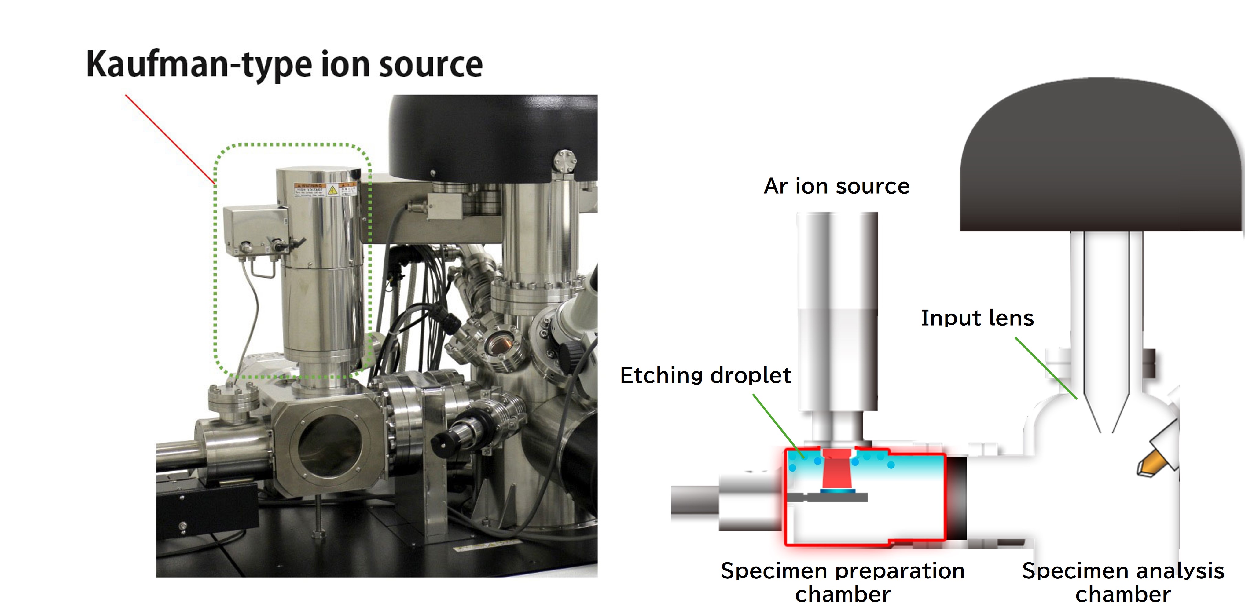
The JPS-9030 installs a Kaufman-type ion source as an Ar ion source. As it allows for a large electric current, practical etching can be performed even at low accelerating voltage. This makes it possible to perform etching while keeping the specimen structure.
The JPS-9030 has its ion source placed in the specimen preparation chamber, limiting contamination caused by etching within the specimen preparation chamber, thus preventing the analysis chamber which keeps the ultra-high vacuum from contamination.
〇Example of utilizing a Kaufman-type ion source-Mo/Si multi-layer film mirror for EUV lithography
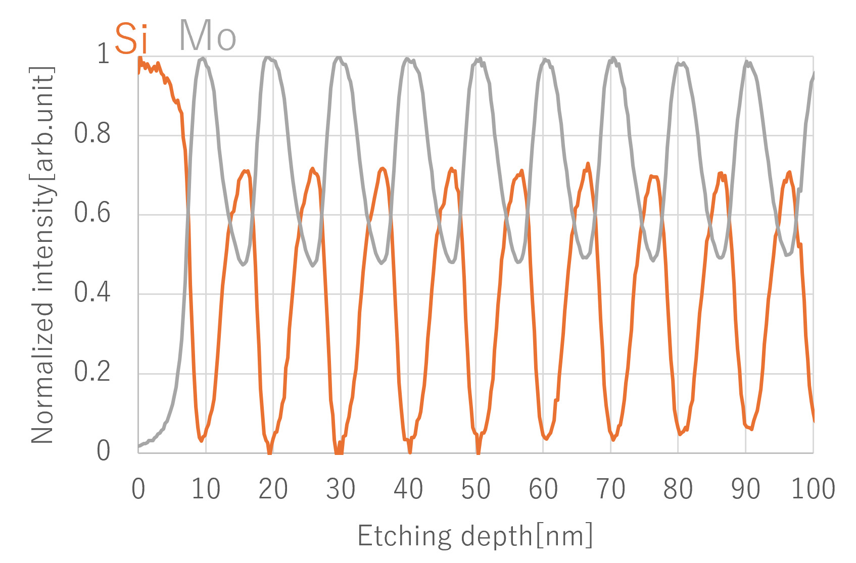
The JPS-9030 can irradiate Ar ions of low acceleration from a vertical direction from the specimen. It can be used for depth profile analysis of ultra-thin multi-layer film. The following shows the depth profile analysis results of Mo/Si multi-layer film mirror for EUV lithography.
It is possible to evaluate a thin film of about 10nm/layer by grabbing the layer structure and evaluating the sharpness of the interface.
③Instrument configuration enabling measurement of a wide range of materials – Other various attachments-
The JPS-9030 provides a variety of options. Moreover, we are prepared to produce attachments according to the request of our users.
A wealth of options
Monochromatic X-ray source that can improve energy resolution
Ar gas cluster ion source which is suitable for easily damaged organic specimens
Infrared heating system rises temperature up to 1,000°C
Transfer vessel which supports air-isolated transfer of a specimen
As above, a wealth of options are available, to respond to any needs of customers.
What can be done with an XPS
Examples of analysis (application) by using an XPS are as follows.
Elemental analysis of the top surface
XPS enables elemental analysis of the top surface of a specimen (10nm or lower).
Therefore, it is possible to easily analyze an organic contaminant that is difficult to determine by appearance.
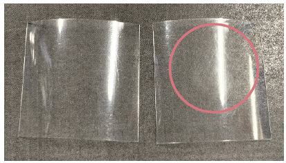
PET(left) and PET contaminated with silicon on the surface(right)
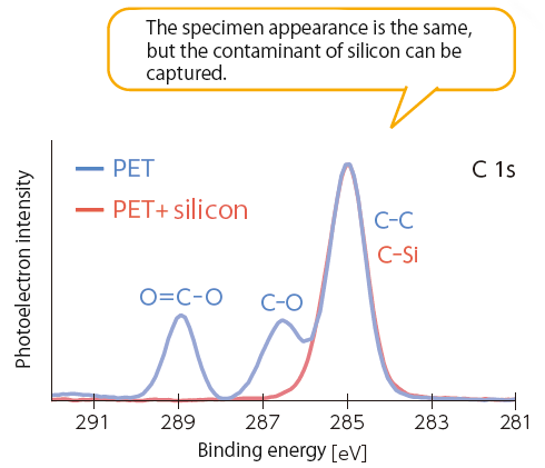
C 1s spectra of PET, PET with silicon
Chemical bonding state analysis
In addition to elemental analysis, XPS can perform a chemical bonding state analysis.
For instance, with a lithium-ion battery, it is possible to evaluate the type of compound for the Li existing on the electrode.
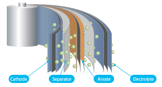
Structure of lithium ion battery
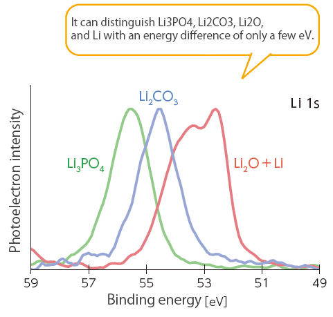
Li 1s spectra of various Li compounds
Depth profile analysis
By performing depth profile analysis using an XPS, it is possible to evaluate the layer structure of a very thin specimen of about 10nm to a specimen of several μm thickness and the chemical bonding state at the interfaces.
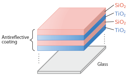
Schematic diagram of antireflective coating on glass surface
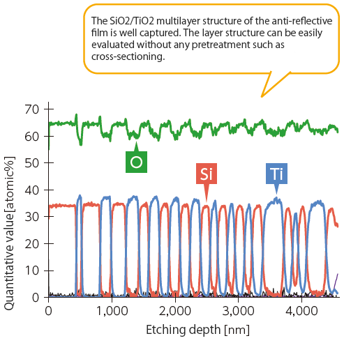
Depth profile analysis result of antireflective coating
Research Publications Using JPS-9030
Specifications
| Intensity
(Mg Kα, 300W equivalent) |
1,000,000 cps or more (Energy resolution (FWHM) for Ag 3d5/2 1.00 eV or less) |
|---|---|
| X-ray source | Maximum accelerating voltage and emission current: 12kV, 50 mA, Mg/Al twin target |
| Illumination lens | Three-stage cylindrical electrostatic lens |
| Energy analyzer | Electrostatic hemispherical analyzer |
| Energy sweep method | Constant Analyzer Energy method Constant Retarding Ratio method |
| Detector | Multi-channel plate |
| Etching ion source | High speed Kaufman-type |
| Ultimate pressure | 7×10⁻⁸ Pa or lower |
Catalogue Download
JPS-9030 Photoelectron Spectrometer
Application
Application JPS-9030
MALDI Application: Analysis of organic thin films
Gallery
More Info
Are you a medical professional or personnel engaged in medical care?
No
Please be reminded that these pages are not intended to provide the general public with information about the products.