Release of Schottky Field Emission Scanning Electron Microscope JSM-IT800(i)/(is) versions −FE-SEM with Intelligence Technology (IT) Platform−
Release Date: 2021/08/31
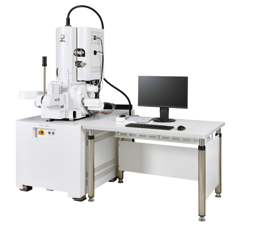
JEOL (President and COO: Izumi Oi) announced that it has developed semi-in-lens versions (i)/(is) which are optimal for the observation of semiconductor devices of the Schottky Field Emission Electron Microscope JSM-IT800 (launched in May 2020), and began selling them in August 2021.
Development Background
Scanning electron microscopes (SEMs) are used in a wide range of fields, such as nanotechnology, metals, semiconductors, ceramics, medicine, and biology. As SEM applications are expanding to not only cover research and development, but also address quality control and product inspection at manufacturing sites, SEM users are in need of fast high-quality data acquisition, as well as simple compositional information confirmation with seamless analytical operation.
To meet these demands, the JSM-IT800 incorporates our In-lens Schottky Plus field emission electron gun for high resolution imaging, and an innovative electron optical control system "Neo Engine", as well as a system of seamless GUI "SEM Center" for fast elemental mapping with a fully embedded JEOL energy dispersive X-ray spectrometer (EDS), as a common platform. Furthermore, the JSM-IT800 allows for the replacement of the objective lens of the SEM as a module, offering different versions to satisfy various users requirements.
The JSM-IT800 is available in five versions with different objective lenses: a hybrid lens version (HL), which is a general-purpose FE-SEM; a super hybrid lens version (SHL/SHLs, two versions with different functions), which enables higher resolution observation and analysis; and the newly-developed semi-in-lens version (i/is, two versions with different functions), which is suited for the observation of semiconductor devices.
The JSM-IT800 can also be equipped with a new Scintillator Backscattered Electron Detector (SBED). The SBED enables easy observation of live images with high responsiveness and produces sharp material contrast even at a low accelerating voltage.
Main Feature
- In-lens Schottky Plus field emission electron gun
Enhanced integration of the electron gun and low-aberration condenser lens provides higher brightness. An ample probe current is available at a low accelerating voltage (100 nA at 5 kV). The unique In-lens Schottky Plus system allows for a variety of applications, from high resolution imaging to fast elemental mapping, and electron backscatter diffraction (EBSD) analysis. - Neo Engine (New Electron Optical Engine)
Neo Engine is a cutting-edge electron optical system that accumulates many years of JEOL core technologies. Users can perform a stable observation even when changing different observation or analytical conditions. High operability for automatic functions is greatly enhanced. - SEM Center / EDS Integration
A GUI "SEM Center" fully integrates with SEM imaging and EDS analysis for providing seamless and intuitive operations. The JSM-IT800 can be enhanced by incorporating optional software add-ons, such as SMILENAVI to assist and provide a learning path for novice users and the LIVE-AI filter (Live Image Visual Enhancer – AI) to acquire a higher quality of live images. - Semi-in-lens versions(i/is)
A semi-in-lens achieves ultra high resolution by converging electron beams with the strong magnetic field lens formed below the objective lens. Moreover, the system efficiently collects the low energy secondary electrons emitted from a specimen and detects the electrons with the upper in-lens detector (UID). Thus, it enables high resolution observation and analysis of tilted specimens and cross-sectional specimens, which are required for failure analysis of semiconductor devices. In addition, it is very useful for voltage contrast observation. - Upper electron detector (UED)
An upper electron detector can be mounted above the objective lens. The advantage of the system is the ability of acquisition of backscattered electron image, and acquisition of secondary electron image in combination with specimen bias. The electrons emitted from a specimen are selected by an UID filer inside the objective lens. UED and UIT allow multiple information to be acquired in a single scan. - New Backscattered Electron Detector
The scintillator backscattered electron detector (SBED, optional) has high responsiveness and is suitable to acquire material-contrast images at a low accelerating voltage.
Main Specifications
| JSM-IT800i version | JSM-IT800is version | |
|---|---|---|
| Resolution (1 kV) | 0.7 nm | 1.0 nm |
| Resolution (15 kV) | 0.5 nm | 0.6 nm |
| Accelerating voltage | 0.01 - 30 kV | |
| Standard detector | Secondary Electron Detector (SED) Upper In-lens Detector (UID) Upper Electron Detector (UED) |
Secondary Electron Detector (SED) Upper In-lens Detector (UID) |
| Electron gun | In-lens Schottky Plus field emission electron gun | |
| Probe current | A few pA to 500 nA (30 kV) | A few pA to 300 nA (30 kV) |
| A few pA to 100 nA (5 kV) | ||
| Objective lens | Semi-in-lens | |
| Specimen stage | Full eucentric goniometer stage | |
| Stage movement | Type1(standard) X; 70 mm Y; 50 mm Z; 1 to 41 mm Type2 (optional) X; 100 mm Y; 100 mm Z; 1 to 50 mm Type3 (optional) X; 140 mm Y; 80 mm Z; 1 to 41 mm Tilt; -5 to 70° Rotation; 360° |
|
| EDS detector | Energy resolution: 133 eV or better Detectable elements Be to U Detection area: 60 mm2 |
|
Sales target
JSM-IT800i version: 5 units/yearJSM-IT800is version: 40 units/year
Link
Are you a medical professional or personnel engaged in medical care?
No
Please be reminded that these pages are not intended to provide the general public with information about the products.