
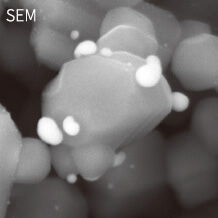
JEOL JSM-IT800 Schottky Field Emission Scanning Electron Microscope
The JSM-IT800, Schottky Field Emission Scanning Electron Microscope with a JEOL Energy Dispersive X-ray Spectrometer(EDS) as standard, is fully integrated with a new GUI "SEM Center", enabling Nonstop acquisition of data from observation to elemental analysis.
Advanced and integrated high peroformance and ease-of-use has improved the work efficiency by more than 50%, making the daily measurement high-throughput.
FEATURE1
FEATURE 1
Hybrid Lens Version(HL)/Super Hybrid Lens Version(SHL)
Based on a combination of the electrostatic and electromagnetic-field lens, two types of objective lens versions are available. The different configurations allow for a wider variety of needs of users to be met, achieving high spatial resolution imaging and analysis of a broad range of samples, from magnetic materials to insulators, while maintaining the same features of the JSM-IT800.

FEATURE2
FEATURE 2
Detection System in JSM-IT800〈SHL〉

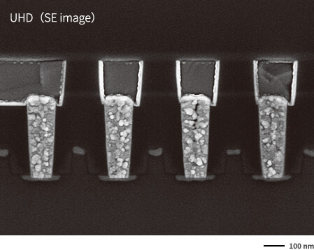
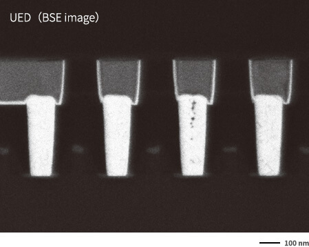
Specimen: section of IC-chip (surface-ethcing, osmium coating), Accelerating voltage: 5.0 kV (without BD mode), Observation mode: SHL, Detector: UHD,UED (BSE mode)
The SE image can be obtained by using the UHD; and the BSE image can be obtained by using the UED.
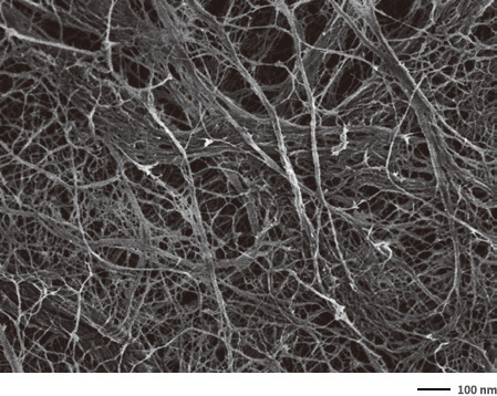
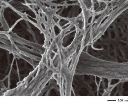
Specimen: Cellulose Nanofiber (CNF), Accelerating voltage: 0.2 kV, Observation mode: BD, Detector: UHD+UED (signal addition)
Specimen courtesy: Prefessor Hiroyuki Yano (Research Institute fro Sustainable Humanosphere, Kyoto University, Japan)
Even the specimen is an organic fiber, the observation is also feasible through controlling the beam damage on the organic fiber.
FEATURE3
FEATURE 3
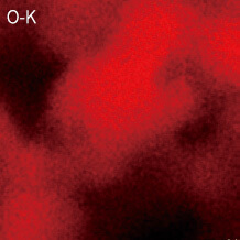
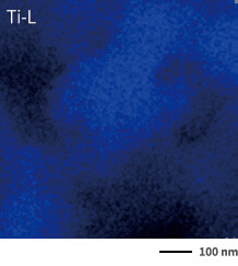
EDS Mapping with JSM-IT800
In addition to BED (normal BSE detector), SBED (scintillator BSE detector) and VBED (versatile BSE detector) are also available to install.
SBED(Scintillator BSE Detector)
The responsibility and sensitivity of the detector are enhanced when substituting semiconductor elements with scintillator in the detector.
-
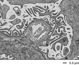
Specimen: ultra thin section of mouse kidney (contrast reversion)
Accelerating voltage: 5.0 kV
Scan speed: 0.04 μsec/pixel (5120×3840 )Observe the biological ultra thin
section through high speed scanning -
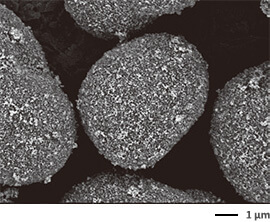
Specimen: toner
Accelerating voltage: 1.5 kVObtain the compositional image
at low accelerating voltage -
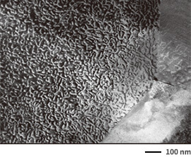
Specimen: steel plate (for observing dislocation)
Accelerating voltage: 25.0 kVObtain the dislocation image at high
accelerating voltage
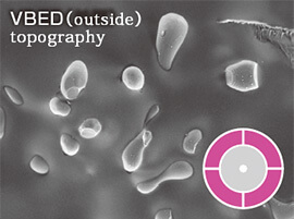
VBED(Versatile BSE Detector)
The semiconductor detection elements are divided into 5 sections. According to the purpose of observation, the signals are selectively obtained from different detection area of these 5 sections.
Angle selection
-
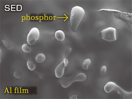
Specimen: phosphor, Accelerating voltage: 3.0 kV
-
-
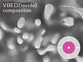
According to the different detection angles of BSE, the compositional information is principally obtained through the inside detecting
elements of VBED and the topographic information is principally obtained through the outside detecting elements. In addition, it is
remarkable that the phosphors under the Al film are bright when using the inside elements of detector to observe .

3-dimensional images can be reconstructed by using these 2-dimensional images obtained from 4 directions.
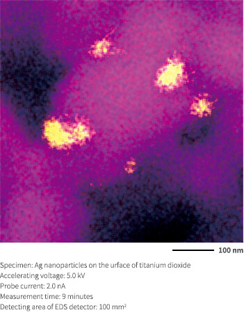
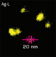
High spatial resolution EDS maps
Even the size of Ag nanoparticles is small to tens of nanometers, the elemental mapping also can make them visible.
Specimen Exchange System
Draw-out system suitable for large-specimen exchange

Optical image acquisition supports both specimen exchange systems
Specimen exchange chamber enabling fast and clean specimen loading/unloading
