Gather-X JED Series
DrySD™ Windowless EDS
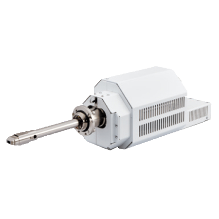
Explore Science with the Windowless EDS Analysis
Stress-free EDS analysis from light to heavy elements!
Driven by carbon neutrality, material development is becoming more important.
For example, in battery materials, a wide range of analysis is required from light elements such as Li to transition metals including Ni, Co, and Mn.
The needs for efficient and highly sensitive analysis are increasing in the analysis of semiconductor materials and nanoparticles of catalysts.
The newly developed DrySD™ Gather-X is a Windowless type EDS that is installable to Schottky Field Emission
Scanning Electron Microscope (FE-SEM). High sensitivity X-ray analysis is possible in all energy bands including low energy characteristic X-rays such as Li-K (54eV). In addition, the safety function interlocked with the SEM/EDS integration software can provide safe and comfortable operability just to anyone.
Features
High sensitivity analysis for all energy regions
Detection of characteristic X-rays less than 100 eV (soft X-ray regions)
Windowless EDS makes it possible to greatly improve detection sensitivity for characteristic X-rays less than 1 keV, and also to detect soft X-ray regions less than 100 eV (Li-K, etc.).
Analysis example of anode material for solid-state lithium-ion battery
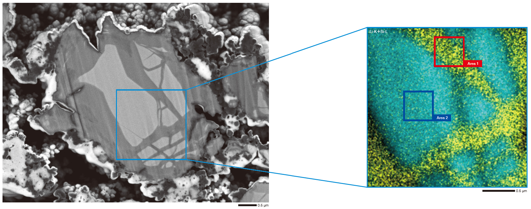
Specimen: Si anode for all solid-state lithium-ion battery
Analysis conditions: Accelerating voltage 3 kV, WD 7 mm,
Probe current 0.6 nA, Measurement time 15 min.
SEM: JSM-IT800 <SHL>
Specimen courtesy:
Professor Atsunori Matsuda
Dept. of Electrical and Electronic Information Engineering,
Toyohashi Univ. of Technology
EDS maps of lithium (Li-K: 54 eV) and silicon (Si-L: 90 eV). Since two spectral peaks with their X-ray energies close to each other, are separated and mapped, the maps revealed the distribution of lithium and silicon on the silicon anode.
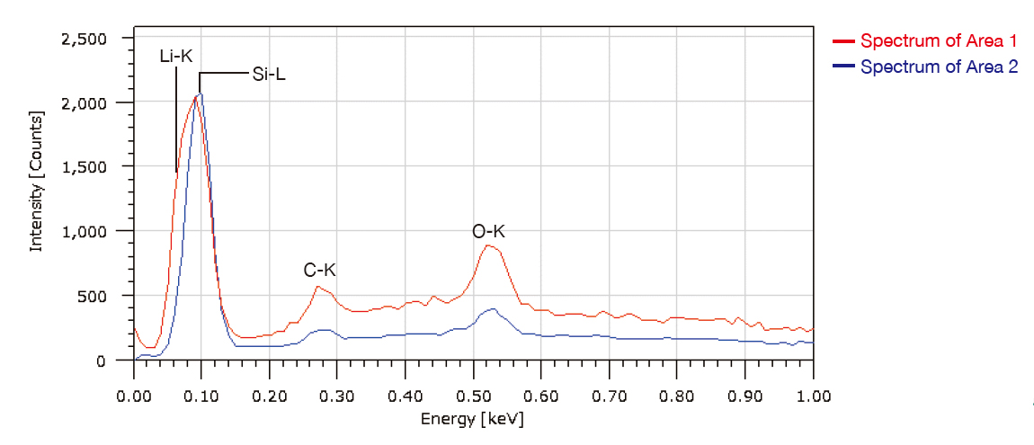

High capability of detecting X-rays less than 100 eV is the largest feature of Windowless EDS.

Large solid angle
The large solid angle enables EDS analysis with high count rates. This advantage leads to a greatly-shortened measurement time and a highly-suppressed electron beam damage to the specimen.
Analysis example of cathode material for lithium-ion battery
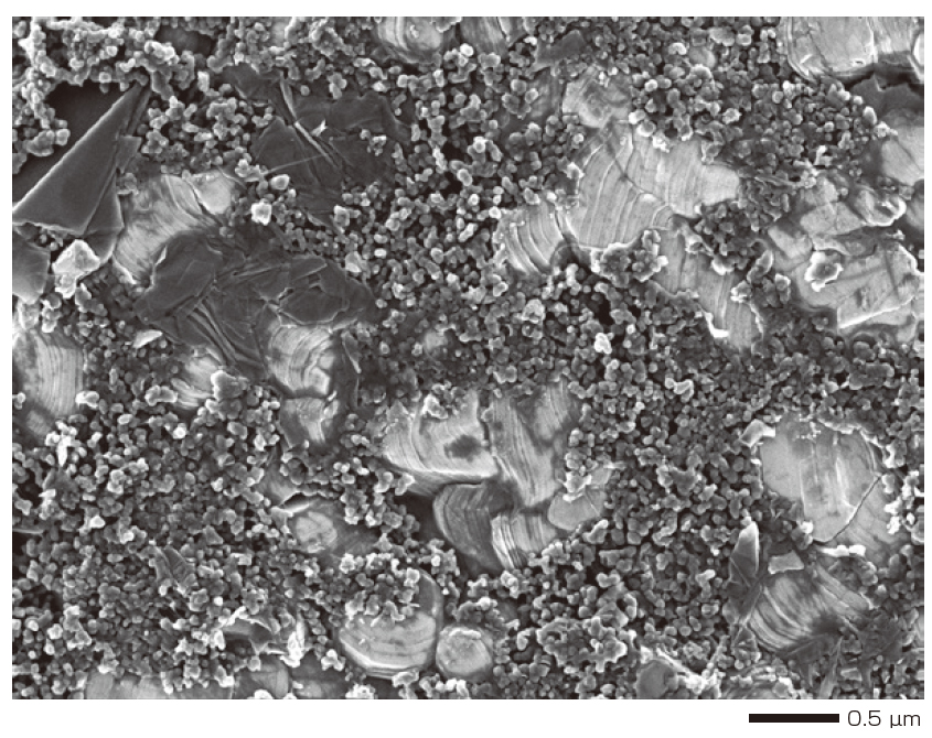
Specimen: Cathode material for lithium-ion battery
Analysis conditions: Accelerating voltage 1.5 kV, (bias to specimen: –5 kV),
WD 7 mm, Probe current 4.8 nA, Measurement time 13 min.
SEM: JSM-IT800 <SHL>
EDS maps of active materials of manganese (Mn), cobalt (Co), nickel (Ni) and oxygen (O), an electron conductive assistant of carbon (C), and a binder of fluorine (F).
These materials are sensitive to electron beam damage and binders are distributed on the specimen surface. EDS maps were performed at a low accelerating voltage (1.5 kV).

Compared to the standard EDS (DrySD™ 100 mm2), X-ray counts are higher in the Windowless EDS, thus improving the peak separation accuracy. The high counts enabled us to acquire more clear, more accurate distribution of fluorine.
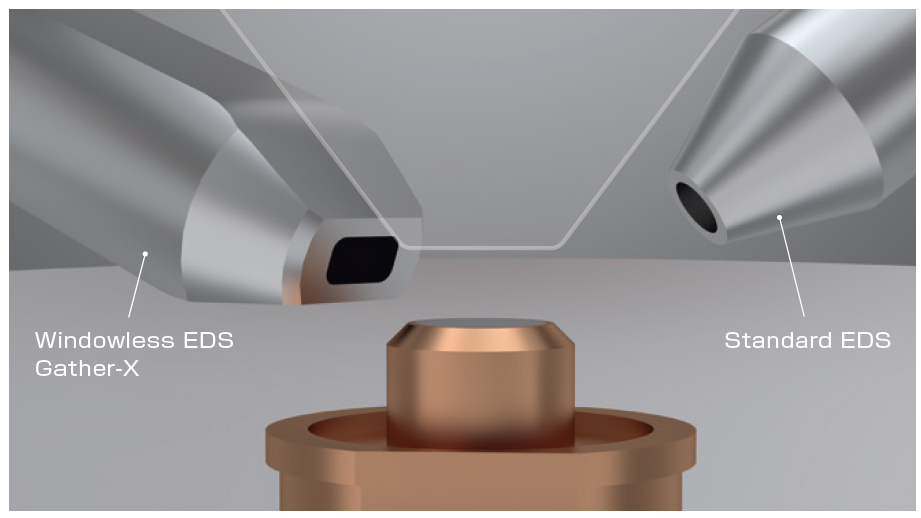

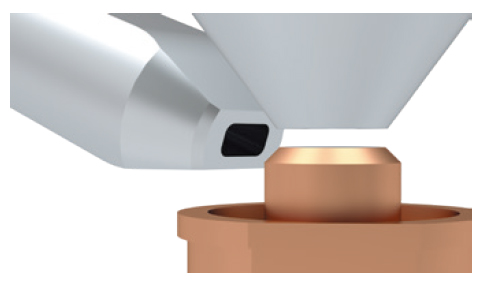
A racetrack-shaped X-ray sensor makes the detector closer to the specimen, achieving a large solid angle.

Analysis at high accelerating voltage
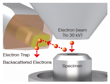
The Electron Trap system, which prevents the backscattered electrons from the specimen to enter the X-ray sensor, enables qualitative and quantitative analysis even at a high voltage of 30 kV.
Analysis example of STEM / EDS for semiconductor
STEM / EDS analysis of a semiconductor material at an accelerating voltage of 30 kV.
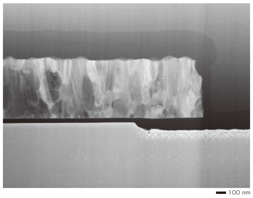

Since the backscattered electrons are trapped, an increase of background is suppressed and the damage to the X-ray sensor is avoided.
Specimen: FIB-milled lamella of SiC power semiconductor
Analysis conditions: Accelerating voltage 30 kV, WD 8 mm,
Probe current 4.1 nA, Measurement time 5 min.
SEM: JSM-IT800 <SHL>*1
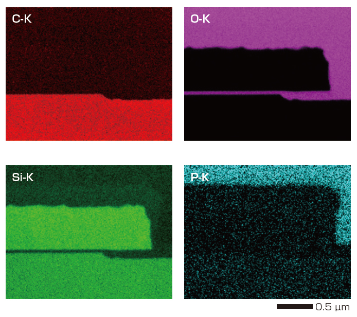
STEM detector of Deben is used.
EDS phase analysis software is optional.
●EDS phase map
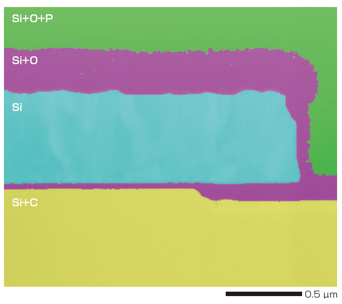

EDS phase analysis software*2 makes it possible to identify the respective phases in the specimen, which distinguishes compounds of multiple elements (not limited to element by element).
High spatial resolution Map
Short WD / BD mode analysis
Qualitative analysis at shorter WD than the standard WD (7 mm), together with a combined use of BD mode which applies a bias voltage to the specimen stage, enables acquisition of high spatial-resolution EDS map at a low accelerating voltage.
Analysis example of catalysts (nanoparticles)
EDS maps of silver (Ag) nanoparticles (size 18 nm) on titanium oxide, observed at ×200,000.
High spatial-resolution EDS maps are effective for analysis of fine particles, such as catalyst particles.
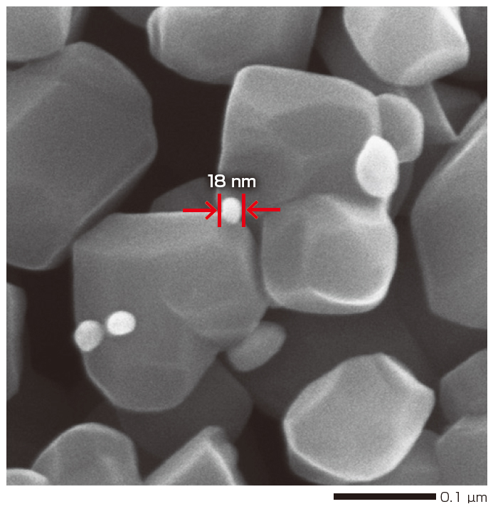
Specimen: Ag nanoparticles on titanium oxide
Analysis conditions: Accelerating voltage 5 kV, (bias to specimen: –5 kV),
WD 4 mm, Probe current 1 nA, Measurement time 9 min.
SEM: JSM-IT800 <SHL>
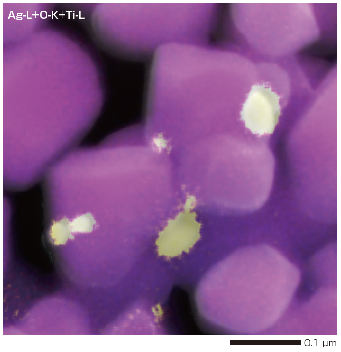
Cream color: Ag-L Purple color: O-K + Ti-L

This feature shows the maximum power of the SEM for excellent EDS analysis.
High operability

EDS integration
You can operate the Windowless EDS with SEM control software (SEM Center). Seamless operations from SEM observation to EDS analysis with Gather-X can be done.
EDS analysis (point, area, MAP, line) on the SEM Center monitor screen can be executed.
Screening functions are also extensive, including Live Analysis and Live MAP.
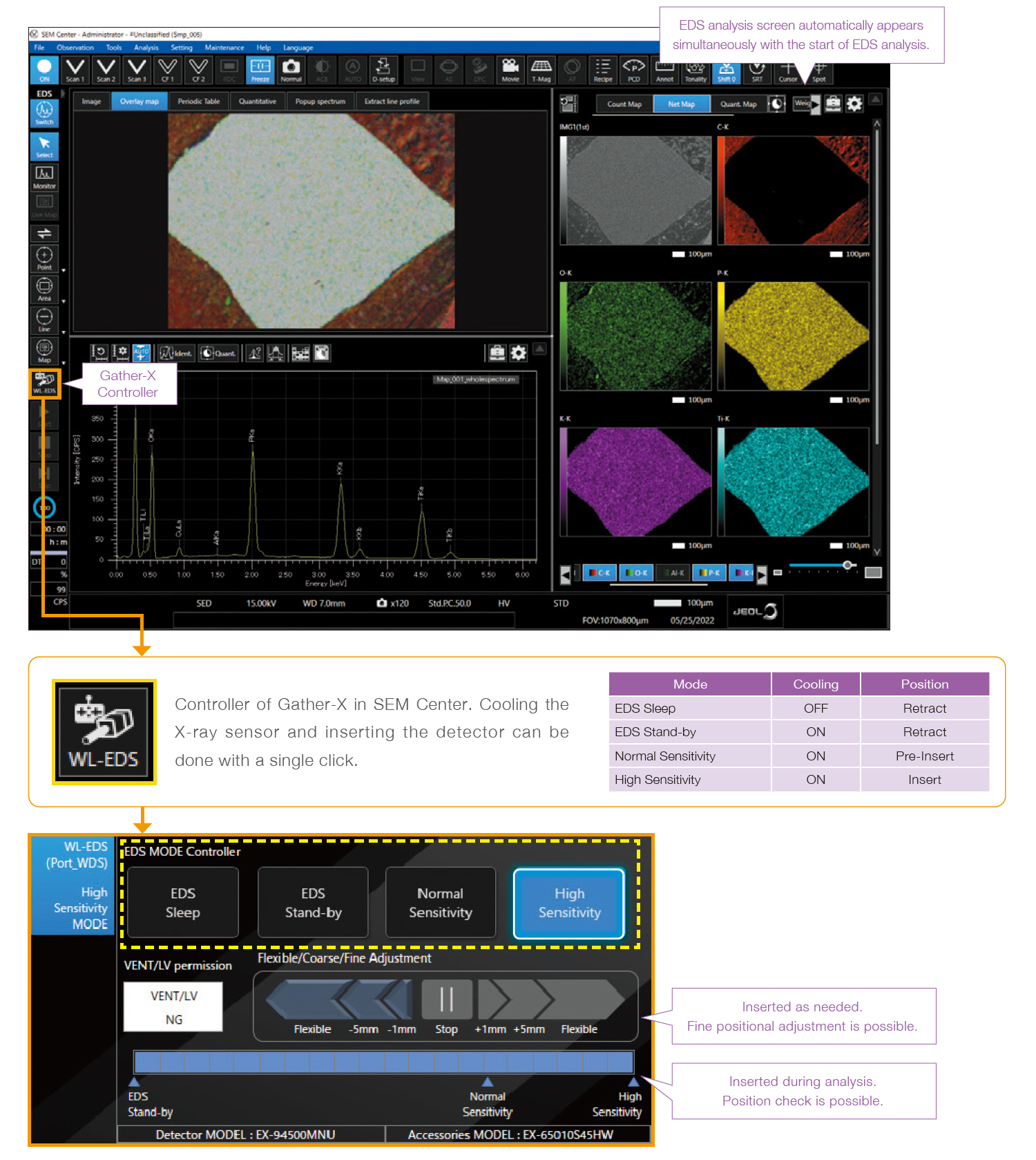

Safety systems linked with the SEM
JEOL, as an electron microscope manufacturer implementing the safety system technologies, provides safe operations through a safety linkage with the SEM and Gather-X.
X-ray sensor protection system
The safety system prevents damage to the cooled X-ray sensor, due to exposure of the X-ray sensor to air.
When the X-ray sensor is being cooled, the vacuum level of the SEM specimen chamber is restricted.
Collision prevention system with SEM stage
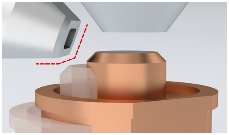
The system prevents the collision of the detector with various holders at the insertion position. Stage movement is restricted depending on the size of the specimen holder. Thus, safe analysis is provided.
Collision prevention system for various optional attachments
The system prevents the collision of the detector with various options attached to the SEM. If an optional attachment is located at a position where it could collide with the detector inserted, the insertion position of Gather-X is automatically restricted.
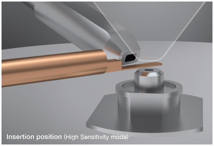
When Gather-X will not collide with the inserted attachment,
analysis can be performed at the insertion position of Gather-X.
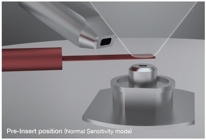
In order to prevent a collision with the inserted attachment,
the insertion position of Gather-X is restricted.
Specifications
| Detectable elements | Li to U |
|---|---|
| Energy resolution | 129 eV or less (Mn-Kα) 59 eV or less (C-Kα) |
| X-ray sensor type | SDD type |
| X-ray sensor size | 100 mm2 |
| Landing voltage | 30 kV or less |
| Vacuum mode | High vacuum mode |
| X-ray sensor cooling | Peltier cooling |
| Drive system | Motor drive |
| Safety system | X-ray sensor protection system linked with the vacuum of SEM ( X-ray sensor is cooled only at the high vacuum mode ) Collision prevention system with the stage and various attachments |
| Gather-X control | Built into SEM control software |
| Applicable models | Schottky Field Emission Scanning Electron Microscope (FE-SEM) |
| Installation requirements |
Room temperature: 20±5 ℃ Humidity: 60% or less (no condensation) |
| Multiple detectors | Possible to configure with Standard EDS |
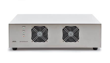
Catalogue Download
Gather-X JED Series DrySD™ Windowless EDS
Related Products
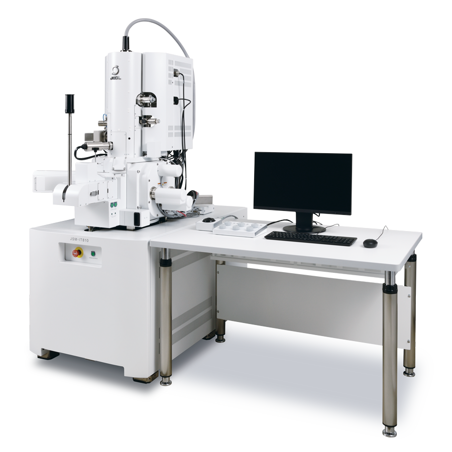
JSM-IT810 Schottky Field Emission Scanning Electron Microscope
Versatility and high spatial resolution meet automation with the JSM-IT810 series FE-SEM.No-coding automation for imaging and EDS analysis is built-in for a streamlined and efficient workflow.New functions are available to ensure high quality data and an enhanced user experience for all SEM users.Functions include the SEM automatic adjustment package, a trapezoidal correction function (useful for EBSD measurements) and Live 3D surface reconstruction for observation of surface topography.Operating a FE SEM has never been easier with the JSM-IT810 series.
More Info
Are you a medical professional or personnel engaged in medical care?
No
Please be reminded that these pages are not intended to provide the general public with information about the products.
