【DISCONTINUED】JSM-7200F Schottky Field Emission Scanning Electron Microscope
DISCONTINUED
This product is no longer available.
If you would like to know the latest information about your preferred product or to find out more about alternatives, please click on the link below. We hope you will continue to use our products.
JSM-7200F has much higher spatial resolution than the conventional models at both high and low accelerating voltages by applying the technology used for “In-Lens SchottkyPlus”, the electron optics equipped on our flagship-model, JSM-7800FPRIME, and by incorporating TTLS (Through-The-Lens System). The maximum probe current of 300 nA is also guaranteed because of the above mentioned features. Thus, JSM-7200F is a next-generation multi-purpose FE-SEM that has capability of high resolution observation, high throughput analysis, ease of use, and expandability.
Features
The main features of JSM-7200F are "In-Lens SchottkyPlus" technology-based electron optics, GB (Gentle Beam mode), TTLS (Through-The-Lens System) that enables high resolution observation at low accelerating voltage and control the amount of low-energy signals to be detected by the upper detectors, and a hybrid objective lens that combines magnetic-lens and electrostatic-lens.
In-Lens Schottky Electron Gun
The In-Lens Schottky electron gun (JEOL patented) has been developed by optimizing the geometry of the electron gun and the low-aberration condenser lens. By this unique technology the electrons emitted from the electron gun can be utilized efficiently than the conventional one, so smaller-diameter of electron probe even with large current is possible. Thus, JSM-7200F is capable of high throughput analysis (EDS, WDS, EBSD, etc.).
TTLS (through-the-lens system)
TTLS (through-the-lens system) is a system that enables high resolution observation at low accelerating voltage and also selection of different signals generated from the specimen by using GB (Gentle Beam mode).
By applying bias voltage to the specimen with GB (Gentle Beam mode), the incident electrons are decelerated and the electrons emitted from the specimen are accelerated, so it is possible to have high resolution images with better signal-to-noise ratio even at low accelerating voltage/landing voltage.
The filtering voltage of the energy filter equipped on TTLS enables you to control the amount of secondary electrons to be detected by the upper detectors. Therefore, images of the top surface of the specimen generated only by high-angle backscattered electrons can be observed at low accelerating voltage with the upper electron detector (UED).
Low-energy electrons, which are not detected with UED and pushed away by the filtering voltage, can be also detected with an optional upper secondary electron detector (USD). Thus, JSM-7200F can detect both secondary electron image and backscattered electron image simultaneously.
Hybrid Objective Lens (combination of magnetic-lens and electrostatic-lens)
JSM-7200F adopts a newly-designed objective lens called “hybrid lens”.
The hybrid lens combines a magnetic-lens and an electrostatic-lens in order to reduce aberrations, so it is possible to obtain higher spatial resolution compared with the conventional out-lens. JSM-7200F also keeps the usability of the conventional out-lens, so it is no problem to observe and analyze magnetic samples.
Applications
Data taken by using the hybrid lens and GB (Gentle Beam mode)
The low-aberration hybrid lens and GB (Gentle Beam mode) enables high resolution observation of insulating materials at very low accelerating voltage.
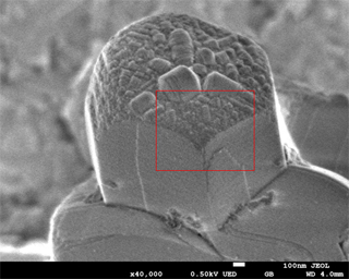
×40,000
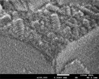
×150,000
Landing voltage: 0.5 kV
Specimen: Mesoporous silica (Courtesy of Professor Shunai Che, Shanghai Jiao Tong University, China)
Data taken by the upper electron detector (UED) with an energy filter
These images are taken by UED at low accelerating voltages. These are high-angle backscattered electron images with composition-rich information, but the image taken at 0.8 kV shows much finer structures of the top surface compared with the image taken at 5 kV. It is necessary to have not only the upper electron detector (UED) but also an energy filter to obtain backscattered electron images of the top surface in order to cut out secondary electrons.
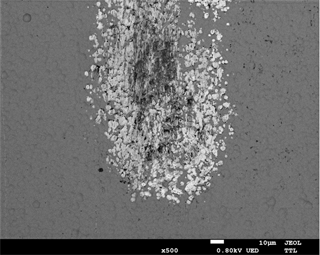
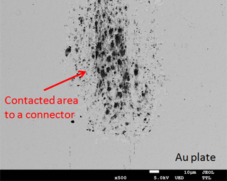
Accelerating voltage: 0.8 kV(to the left), 5kV(to the right)
Energy filter: -250 V
Specimen: The surface of an Au plate
Specifications
| JSM-7200F | JSM-7200F with Low Vacuum mode (LV) * Option | |
| Resolution (1 kV) | 1.6 nm | |
| Resolution (20 kV) | 1.0 nm | |
| Resolution (Analysis) | 3.0 nm
(15 kV, WD:10 mm, probe current:5 nA) |
|
| Magnification | x10 to x1,000,000 | |
| Accelerating voltage | 0.01 to 30 kV | |
| Probe current | 1 pA to 300 nA | |
| Detector (standard) | UED, LED | |
| Detector (optional) | USD, RBED | |
| Electron gun | In-lens Schottky field emission electron gun | |
| Aperture angle control lens | Built in | |
| Objective lens | Conical lens | |
| Specimen stage | Fully eucentric goniometer stage | |
| Stage movement | X: 70 mm, Y: 50 mm, Z: 2 to 41 mm,
Tilt: -5 to 70°, Rotation: 360° |
|
| Motor control | 5 axes motor controlled | |
| Specimen exchange chamber | Maximum diameter : 100 mm
Maximum height : 40 mm (vented with dry nitrogen) |
|
| Large depth of focus (LDF) | Built in | |
| LV mode | - | Built in |
| LV detector | - | LV-BED, LV-SED
(optional) |
| LV resolution | - | 1.8 nm(30 kV) |
| Pressure in LV mode | - | 10 Pa to 300 Pa |
| Orifice control | - | On the operation GUI |
| Introduced gas | Nitrogen | |
| Evacuation system (SIP, TMP) | SIP x 2, TMP | |
| Evacuation system (RP) | RP x 1 | RP x 2 |
Principal Options
Retractable Backscattered electron detector (RBED)
Upper secondary electron detector (USD)
Low vacuum secondary electron detector (LV-SED)
Energy dispersive X-ray spectrometry (EDS)
Electron backscatter diffraction (EBSD)
Wavelength dispersive X-ray spectrometry (WDS)
Large specimen stage (SS100S)
Specimen exchange chamber (Type1)
Stage navigation system (SNS)
Chamber camera
Operation table
SMile View
Soft X-ray Emission Spectrometer(SXES)
Application
Application JSM-7200F
Introducing Cryo Scanning Electron Microscopy
Related Products
Related Products
Soft X-ray Emission Spectrometer (SXES)
The Soft X-Ray Emission Spectrometer (SXES) is an ultra-high resolution spectrometer consisting of a newly-developed diffraction grating and a high-sensitivity X-ray CCD camera.
In the same way as EDS, parallel detection is possible, and 0.3 eV (Fermi-edge, Al-L standard) ultra-high energy resolution analysis can be performed, surpassing the energy resolution of WDS.
miXcroscopy™ Linked Optical & Scanning Electron Microscopy System
The same specimen holder can now be used for both the optical microscope and the scanning electron microscope. As a result, by managing the stage information with dedicated software, it is possible for the system to record the locations observed with the optical microscope, and then further magnify the same areas with the scanning electron microscope to observe the fine structures at higher magnification & higher resolution.The observation targets found with the optical microscope can be seamlessly observed with the scanning electron microscope without having to search for the target again. It is now possible to smoothly and easily compare and verify the optical microscope images and scanning electron microscope images.
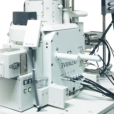
Serial Block-face SEM JSM-7200F・7800F / Gatan 3View®2XP
The 3View®2XP (Gatan Inc.) is incorporated into the Schottky field emission scanning electron microscope that can produce fine electron probe at a high current over long periods of time, making it possible to automatically create cross sections of the specimen and obtain images. The 3D reconstruction of the acquired images enables detailed analysis of the fine structures in three dimensions.
More Info
Are you a medical professional or personnel engaged in medical care?
No
Please be reminded that these pages are not intended to provide the general public with information about the products.