【DISCONTINUED】JSM-F100 Schottky Field Emission Scanning Electron Microscope
DISCONTINUED
This product is no longer available.
If you would like to know the latest information about your preferred product or to find out more about alternatives, please click on the link below. We hope you will continue to use our products.
The JSM-F100 incorporates not only our highly regarded In-lens Schottky Plus field emission electron gun and "Neo Engine" (electron optical control system), but also a new GUI "SEM Center" and an innovative "LIVE-AI (Live Image Visual Enhancer – Artificial Intelligence) filter". This enables an optimal combination of high spatial resolution imaging and high operability. Furthermore, the JSM-F100 comes with a JEOL energy dispersive X-ray spectrometer (EDS), which is fully integrated within "SEM Center" for seamless acquisition from images to elemental analysis results. Inspired by users in pursuing the evolution, and integration, of high performance and operability, the JSM-F100 achieves a superb work efficiency, 50% or higher than that of our previous JSM-7000 series, leading to dramatically increased high throughput capabilities.
Features
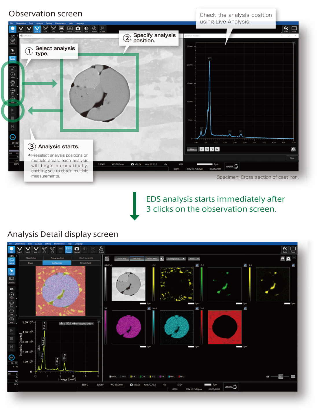
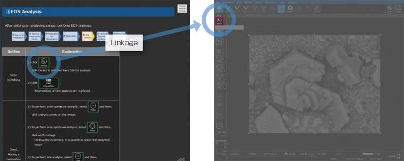
New function of "SEM Center" for integrating EDS
A newly developed operation GUI "SEM Center" fully integrates SEM imaging and EDS analysis. This powerful function provides next-generation operability and high resolution images obtained with FE-SEM.
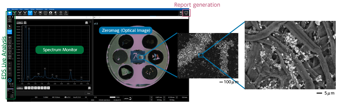
New "Zeromag" function
"Zeromag", incorporated for seamless transition from optical to SEM imaging, makes it easy to locate the target specimen area.
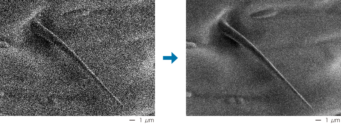
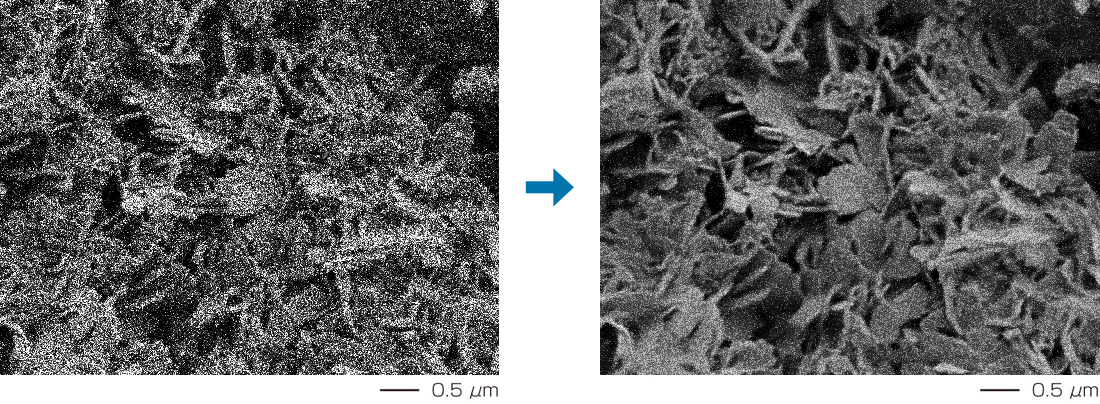
New LIVE-AI filter *Option
Utilizing the AI (artificial intelligence) capability, LIVE-AI filter is incorporated for a higher quality of live images. Unlike image integration processing, this new filter can display a seamless moving live image with no residual image. This unique feature is very effective for quickly searching observation areas, focusing, and stigmator adjustment.
Comparison of normal mode and LIVE-AI filter
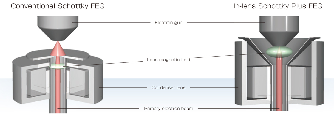
In-lens Schottky Plus field emission electron gun (FEG)
Enhanced integration of the electron gun and low-aberration condenser lens provides higher brightness. Ample probe current is available at low accelerating voltage, supporting various capabilities from high resolution imaging to high speed elemental mapping.
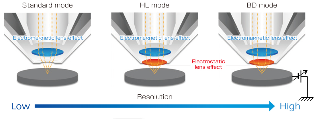
Hybrid Lens (HL)
The Hybrid Lens (HL), a combination of the electrostatic and electromagnetic-field lens, supports high spatial resolution imaging and analysis of various specimens ranging from magnetic materials to insulators.
NeoEngine (New Electron Optical Engine)
Neo Engine, a cutting-edge electron optical control system, achieves a significantly improved precision of automatic functions, as well as a superbly higher operability.
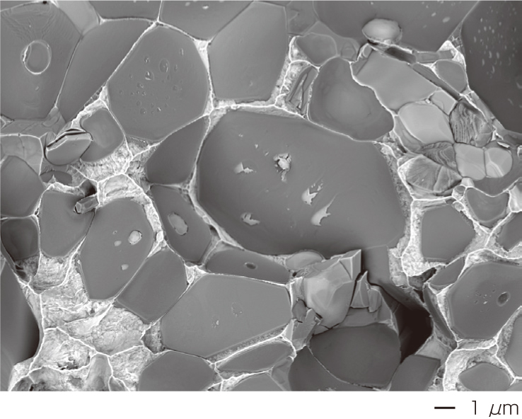
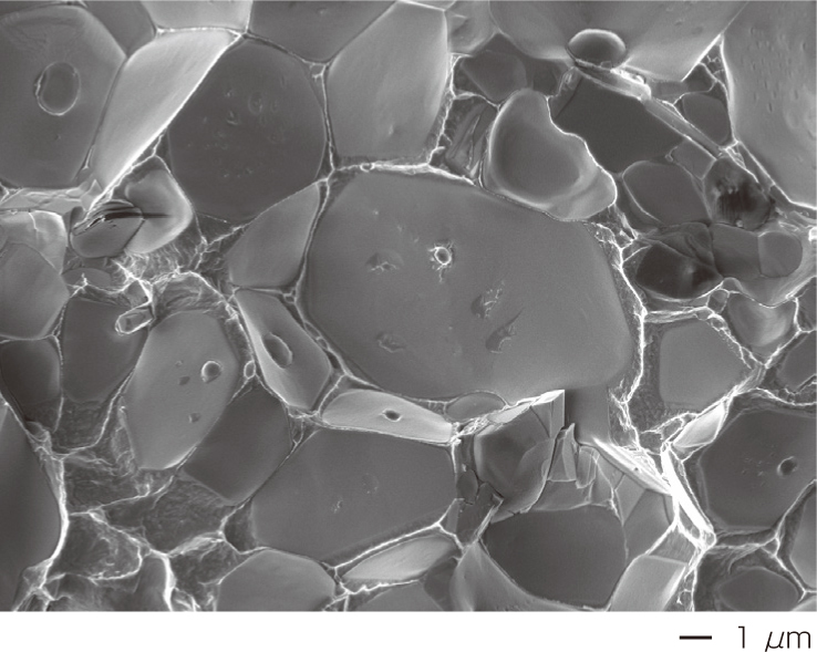
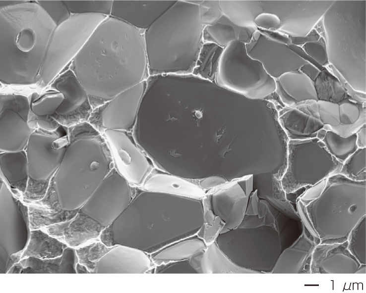
AFS・ACB
Before auto focus adjustment
After auto focus adjustment
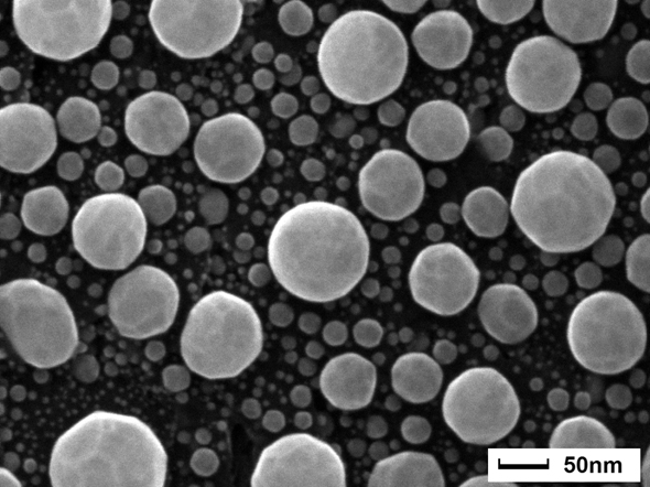
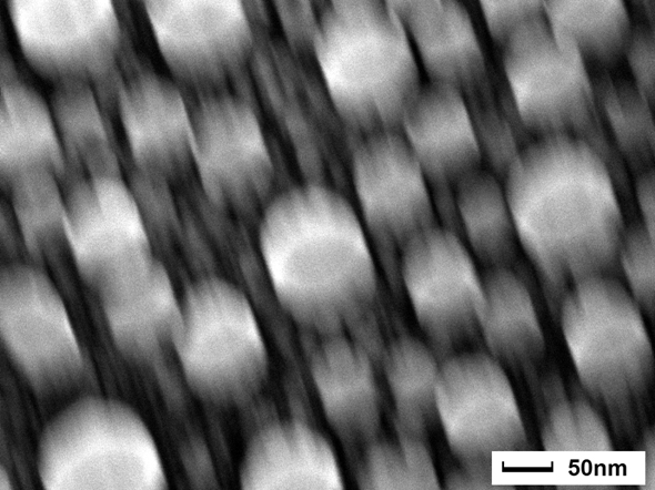
Specimen: Sn nanoparticles on carbon
Accelerating voltage: 15 kV, WD: 2 mm, Observation mode: BD, Detector: UED, Magnification: x200,000
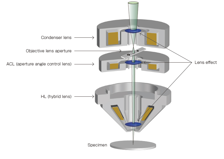
ACL (aperture angle control lens)
The JSM-F100 incorporates an aperture angle control lens (ACL). ACL suppresses the spread of the incident electrons for always maintaining a smallest probe. This is achieved by the optimum control of the aperture angle for large variations of the probe current, enabling smooth SEM operations including high resolution imaging and X-ray analysis. Together with the in-lens Schottky electron gun, ACL is of prime importance for supporting this multipurpose SEM.
Detector system
The JSM-F100 can accommodate four detectors to enable you to simultaneously observe various SEM images uniquely formed by each detector. Like the conventional out-lens SEM, the LED (lower electron detector) and the optional RBED (retractable backscattered electron detector) are available. In addition, the JSM-F100 configures two in-lens detectors of the standard UED (upper electron detector) and the optional USD (upper secondary electron detector). The UED forms an SEM image that mixes secondary electrons and high angle backscattered electrons. The USD detects low energy secondary electrons intercepted by an energy filter just beneath the UED, to form an SEM image.
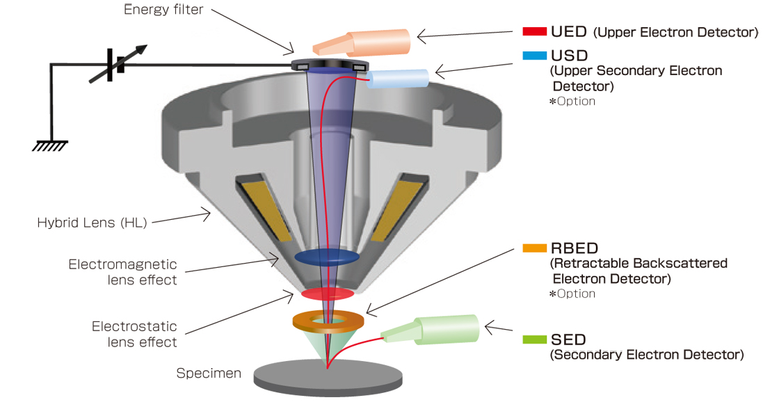
■UED: High-angle backscattered electrons
(compositional & crystalline information)
■RBED: Backscattered electrons
(compositional, crystalline, and topographic information)
■USD: Secondary electrons
(surface morphological information)
■SED: Secondary and backscattered electrons
(topographic information)
SMILE VIEW™ Lab
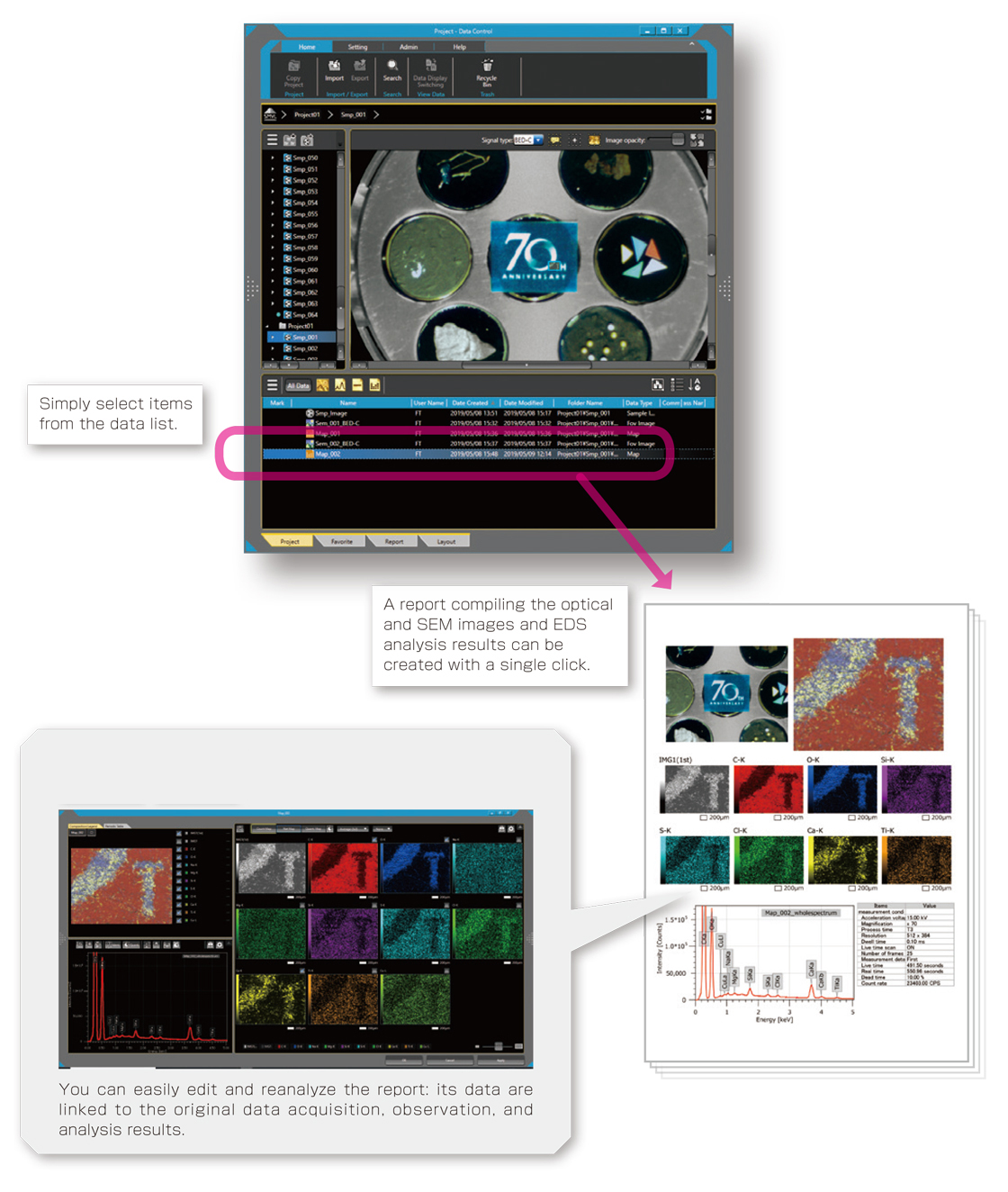
SMILENAVI *Option
SMILENAVI is an assistant tool designed for beginners to allow smooth basic SEM operations. When the operator clicks the appropriate button as indicated by the SMILENAVI flowchart,the SEM GUI is linked to the click operation for operator guidance. Since the GUI displays operation steps and button locations, operators will be able to operate the SEM without using SMILENAVI.
Link
Specifications
Features
| Resolution (1 kV) | 1.3 nm |
|---|---|
| Resolution (20 kV) | 0.9 nm |
| Magnification | Photo magnification : X 10 to X 1,000,000 (128 mm X 96 mm)
Display magnification : X 27 to X 2,740,000 (1,280 X 960 pixels) |
| Accelerating voltage | 0.01 to 30 kV |
| Probe current | A few pA to 300 nA (30 kV)
A few pA to 100 nA (5 kV) |
| Standard Detector | Upper Electron Detector (UED)
Secondary Electron Detector (SED) |
| Electron gun | In-lens Schottky Plus field emission electron gun |
| Aperture angle Control Lens (ACL) | Built-in |
| Objective lens | Hybrid Lens (HL) |
| Specimen stage | Full eucentric goniometer stage |
| Specimen movement | X: 70 mm, Y: 50 mm, Z: 2 to 41 mm
Tilt: -5 to 70°, Rotation: 360° |
| Motor control | 5-axis motor control |
| Specimen size (Draw out) | Maximum diameter: 170 mm
Maximum height: 45 mm (WD 5 mm) |
| Large Depth of Focus (LDF) | Built-in |
| EDS functions | Spectral analysis, Qualitative & Quantitative analysis,
Line analysis (horizontal line, specific direction line), Elemental mapping, Probe tracking, etc. |
Details of DrySDTM detectors 60 mm2 133 eV or less B to U
| Data management function | SMILE VIEW™ Lab |
|---|---|
| Report generation function | SMILE VIEW™ Lab |
Principal Options
Low Vacuum function
Retractable Backscattered Electron Detector (RBED)
Upper Secondary Electron Detector (USD)
Low Vacuum Secondary Electron Detector (LVSED)
Scanning Transmission Electron Detector (STEM)
Electron Backscatter Diffraction System (EBSD)
Wavelength Dispersive X-ray Spectrometer (WDS)
Soft X-ray Emission Spectrometer (SXES)
Cathodoluminescence Detector (CL)
Specimen exchange chamber
Stage navigation system (SNS)
Chamber camera
Operation table
Operation panel
Trackball
SMILENAVI
LIVE-AI filter
SMILE VIEW™ Map
Catalogue Download
JSM-F100 Schottky Field Emission Scanning Electron Microscope
Application
Application JSM-F100
More Info
Are you a medical professional or personnel engaged in medical care?
No
Please be reminded that these pages are not intended to provide the general public with information about the products.