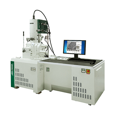
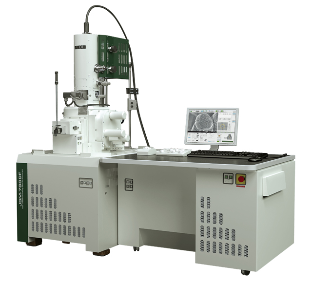
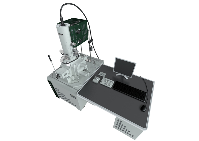
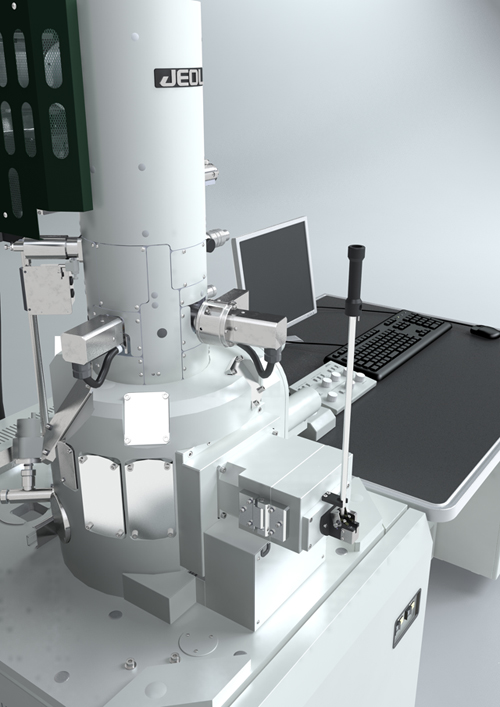
【DISCONTINUED】JSM-7800F Schottky Field Emission Scanning Electron Microscope
DISCONTINUED
This product is no longer available.
If you would like to know the latest information about your preferred product or to find out more about alternatives, please click on the link below. We hope you will continue to use our products.
Features
The newly-developed Super Hybrid Lens (SHL) is used to achieve the next-generation high-resolution SEM, without sacrificing operability. The adoption of the Schottky type electron gun delivers stable analysis with large probe current.
High resolution observation using the Super Hybrid Lens (SHL)
The objective lens is a Super Hybrid Lens (SHL), which consists of an electrostatic magnetic field overlapped with an electrostatic electric field. Reducing the chromatic and spherical aberrations improves the resolution, especially at low accelerating voltages. The SHL does not exert magnetic field influences on the specimen, so observations of magnetic materials and EBSD analysis can be performed without difficulty.
Energy selection at low accelerating voltages
An energy filter is mounted directly below the upper electron detector (UED), so energy selection is possible. Secondary electrons and backscattered electrons can be selected accurately, even at low accelerating voltages, allowing composition observation of the top surface of the specimen using a backscattered electron image at low accelerating voltages.
Top surface imaging using Gentle Beam
By applying a bias voltage to the specimen (GB), the speed of the incident electrons is reduced and the speed of the released electrons is increased. This allows high-resolution images with a good signal-to-noise ratio to be acquired even with low specimen exposure energies. If GB mode is used, which allows a higher bias voltage to be applied, even higher-resolution observations can be made even at specimen exposure energies of just a few tens of eV.
Acquisition of all information using multiple detectors
The JSM-7800F incorporates 4 types of detectors, including an upper electron detector (UED), upper secondary electron detector (USD), backscattered electron detector (BED), and a lower electron detector (LED). For the UED, the secondary electron and backscattered electron dose can be changed according to the filter voltage, making it possible to select the electron energy. The USD detects the low-energy electrons that bounce off the filter. With the BED, channeling contrast can be clearly observed by detecting the low-angle backscattered electrons. The LED enables acquisition of images with a 3-dimensional appearance, including the surface roughness information from the illumination effects.
Application examples
Observation at low accelerating voltage
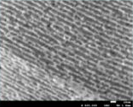
By the Gentle Beam (GB) method, observation from at the specimen exposure energy of 10 eV is possible. The surface of graphene sheet the thickness of just one atom is observable with the specimen exposure energy being set 80 eV.
Specimen: Graphene ( specimen exposure energies: 80eV)
Energy selection
With BE image (left) and SE image (right) simultaneously being obtained by UED and USD, precise interpretation of images is possible. Segregation between gold particles and TiO2, not obvious by SE image which contrast depends mainly on the topography, becomes clear by BE image, where gold particles become brighter because of its higher mean atomic number.
BE image
Spesimen: gold supported TiO2 catalyst (2kV)
SE image
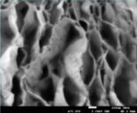
Observation using GBSH
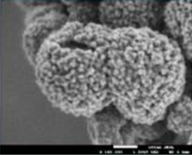
The GBSH method applies a negative voltage to a specimen. With the aberration being reduced, high resolution images are produced. Clear observation of mesoporous silica is realized.
Specimen: Mesoporous silica (specimen exposure energy: 1keV)
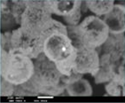
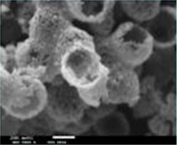
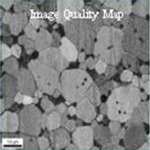
Observation of magnetic materials
SHL does not form magnetic field around a specimen. Threfore high resolution observation of magnetic materials, and even at low specimen exposure energies, can be performed without difficulty.
Specimen: Magnetite nano particles (specimen exposure energy: 1keV)
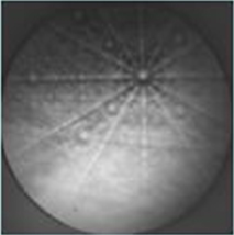
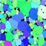
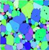
EBSD can be performed comfortably, since SHL does not exert magnetic field influences on the specimen. IPF Map produces high precision crystal orientation analysis.
Number of points: 118585
Dimensions:
X Max: 80.00 microns, Y Max: 79.89 microns
Step: 0.25 microns
Phases: Nd2Fe14B
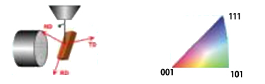
Example of EBSD pattern

ND
TD
RD
Specifications
| Resolution | 0.8 nm(15 kV) 1.2 nm(1 kV) 3.0 nm (15kV、5nA、WD10mm) |
|---|---|
| Magnification | ×25 to ×1,000,000(SEM) |
| Accelerting Voltage | 0.1kV to 30kV |
| Probe current | Several pA to 200nA |
| Aperture angle optimizing lens | Built-in |
| Detectors | Upper Electron Detector(UED) Lower Electron Detector(LED) |
| Energy filter | UED Filter Voltage Change Function built-in |
| Gentle Beam | Built-in |
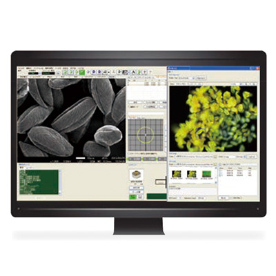
| Image display | Image display area 1,280 x 960 pixel, 800 x 600 pixel |
| Specimen exchange chamber | Standard Specimen Exchange Chamber TYPE2A is composed. |
| Specimen stage | 5-axis motor drive stage Full eucentric goniometer stage |
| X-Y | X:70mm, Y:50mm |
| Tilt | -5 to +70° |
| Rotation | 360° |
| WD | 2mm to 25mm |
| Evacuation system | Two SIPs, TMP, RP |
| Eco design | During normal operation :1.1 kVA During the sleepmode : 0.8 kVA |
Principal Options
Energy Dispersive X-ray Spectrometer (EDS)
Wavelength Dispersive X-ray Spectrometer (WDS)
Electron Backscatter Diffraction (EBSD) System
Cathodoluminescence Detector (CLD)
Application
Application JSM-7800F
Comparison of 3D Imaging Methods in Electron Microscopy for Biomaterials
Application of Scanning Electron Microscope to Dislocation Imaging in Steel
High Angle Backscattered Electrons and Low Angle Backscattered Electrons
Rapid Characterization of Bacteria Using ClairScope and SpiralTOF
Gallery
Related Products
miXcroscopy™ Linked Optical & Scanning Electron Microscopy System
The same specimen holder can now be used for both the optical microscope and the scanning electron microscope. As a result, by managing the stage information with dedicated software, it is possible for the system to record the locations observed with the optical microscope, and then further magnify the same areas with the scanning electron microscope to observe the fine structures at higher magnification & higher resolution.The observation targets found with the optical microscope can be seamlessly observed with the scanning electron microscope without having to search for the target again. It is now possible to smoothly and easily compare and verify the optical microscope images and scanning electron microscope images.
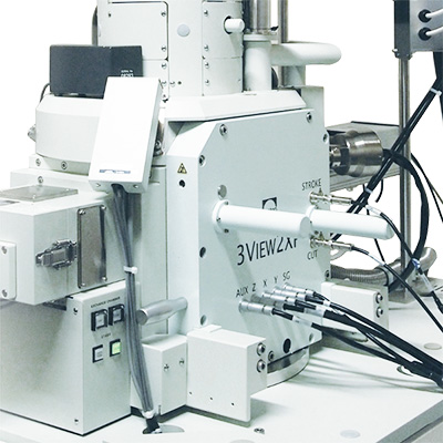
Serial Block-face SEM JSM-7200F・7800F / Gatan 3View®2XP
The 3View®2XP (Gatan Inc.) is incorporated into the Schottky field emission scanning electron microscope that can produce fine electron probe at a high current over long periods of time, making it possible to automatically create cross sections of the specimen and obtain images. The 3D reconstruction of the acquired images enables detailed analysis of the fine structures in three dimensions.
More Info
Are you a medical professional or personnel engaged in medical care?
No
Please be reminded that these pages are not intended to provide the general public with information about the products.