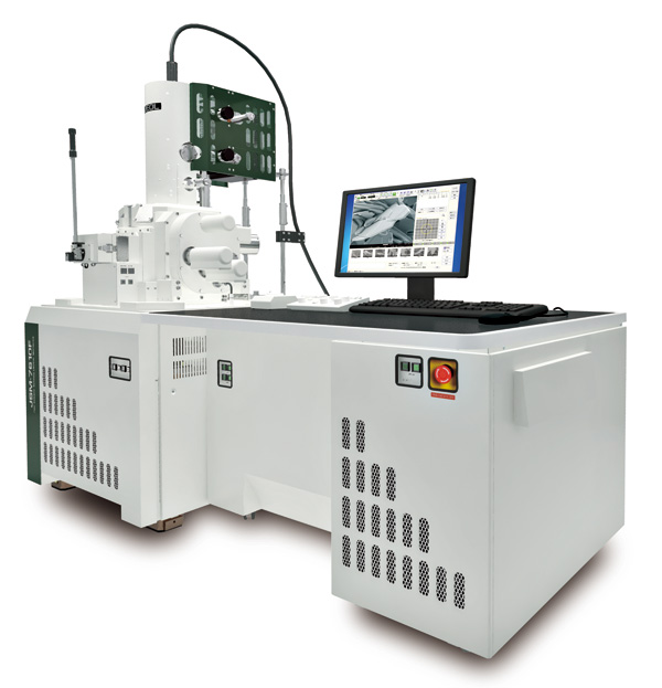
【DISCONTINUED】JSM-7610F Schottky Field Emission Scanning Electron Microscope
DISCONTINUED
This product is no longer available.
If you would like to know the latest information about your preferred product or to find out more about alternatives, please click on the link below. We hope you will continue to use our products.
JSM-7610F is an ultra high resolution Schottky Field Emission Scanning Electron Microscope which has semi-in-lens objective lens. High power optics can provide high throughput and high performance analysis. It’s also suitable for high spatial resolution analysis. Furthermore, Gentle Beam mode can reduce the incident electron penetration to the specimen, enabling you to observe its topmost surface by using a few hundred landing energy.
Features
High resolution imaging and high performance analysis by semi-in-lens objective lens
The JSM-7610F combines two proven technologies – an electron column with semi-in-lens objective lens which can provide high resolution imaging by low accelerating voltage and an in-lens Schottky FEG which can provide stable large probe current – to deliver ultrahigh resolution with wide range of probe currents for all applications (A few pA to more than 200 nA).
The in-lens Schottky FEG is a combination of a Schottky FEG and the first condenser lens and is designed to collect the electrons from the emitter efficiently.
The topmost surface imaging at low accelerating voltage by Gentle Beam mode (GB)
The Gentle Beam (GB) mode applies a negative voltage to a specimen and decelerates incident electrons just before they irradiate the specimen, thus the resolution is improved at an extremely low accelerating voltage.
Therefore, 7610F is possible to observe a topmost surface by a few hundred eV which were difficult to observe conventionally and nonconductive samples such as ceramics and semiconductor etc.
High throughput and high performance analysis by High Power Optics
The High Power Optics produces fine electron probe for both observation and analysis.
The aperture angle control lens maintains a small probe diameter even at a larger probe current.
Using both techniques, the 7610F is suitable for a wide variety of analysis with EDS, WDS, CL etc
Application examples
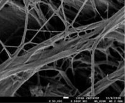
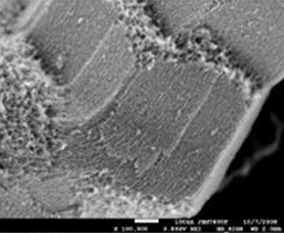
High resolution imaging by semi-in-lens objective lens
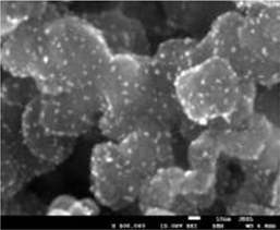
Sample: Pt Catalyst Accelerating Voltage 15 kV
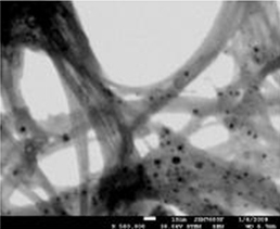
Sample: Carbon Nanotubes Accelerating Voltage 30 kV
High spatial resolution analysis by semi-in-lens objective lens
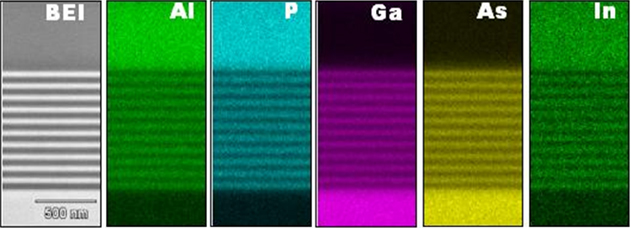
LED cross section (EDS analysis of multilayers below 100 nm)
The topmost surface imaging at ultra low landing energy by Gentle Beam mode (GB)
Sample: filter Landing energy 500 eV
Sample: Mesoporous Silica Landing energy 800 eV
Specifications
| SEI resolution | 1.0nm (15kV) , 1.3nm (1kV) , During analysis 3.0 nm (15 kV、 probe current 5 nA) | ||
|---|---|---|---|
| Magnification | 25 to 1,000,000 | ||
| Accelerating voltage | 0.1kV to 30kV | ||
| Probe current | A few pA to 200nA | ||
| Aperture angle control lens | Built-in | ||
| Detectors | Upper detector, lower detector | ||
| Energy filter | New r-filter | ||
| Gentle Beam | Built-in | ||
| Specimen stage | Eucentric, 5 axes motor control | ||
| Type | Type IA 2 | Type II (Optional) | Type III (Optional) |
| X-Y | 70mm×50mm | 110mm×80mm | 140mm×80mm |
| Tilt | -5° to +70° | -5° to +70° | -5° to +70° |
| Rotation | 360°endless | 360°endless | 360°endless |
| WD | 1.0mm to 40mm | 1.0mm to 40mm | 1.0mm to 40mm |
| Evacuation system | Two SIPs, TMP, RP | ||
Principal Options
Retractable backscatter electron detector (RBEI)
Low angle backscatter electron detector (LABE)
Scanning Transmission Electron Detector (STEM)
Stage navigation system (SNS)
Ion cleaning device
Energy dispersive X-ray spectrometer (EDS)
Wavelength dispersive X-ray spectrometer (WDS)
Cathodoluminescence Detector (CL)
Specimen holder A variety of optional specimen holder are available
Application
Application JSM-7610F
MALDI Application: Analysis of organic thin films
Gallery
-
JSM-7610F
Related Products
miXcroscopy™ Linked Optical & Scanning Electron Microscopy System
The same specimen holder can now be used for both the optical microscope and the scanning electron microscope. As a result, by managing the stage information with dedicated software, it is possible for the system to record the locations observed with the optical microscope, and then further magnify the same areas with the scanning electron microscope to observe the fine structures at higher magnification & higher resolution.The observation targets found with the optical microscope can be seamlessly observed with the scanning electron microscope without having to search for the target again. It is now possible to smoothly and easily compare and verify the optical microscope images and scanning electron microscope images.
More Info
Are you a medical professional or personnel engaged in medical care?
No
Please be reminded that these pages are not intended to provide the general public with information about the products.