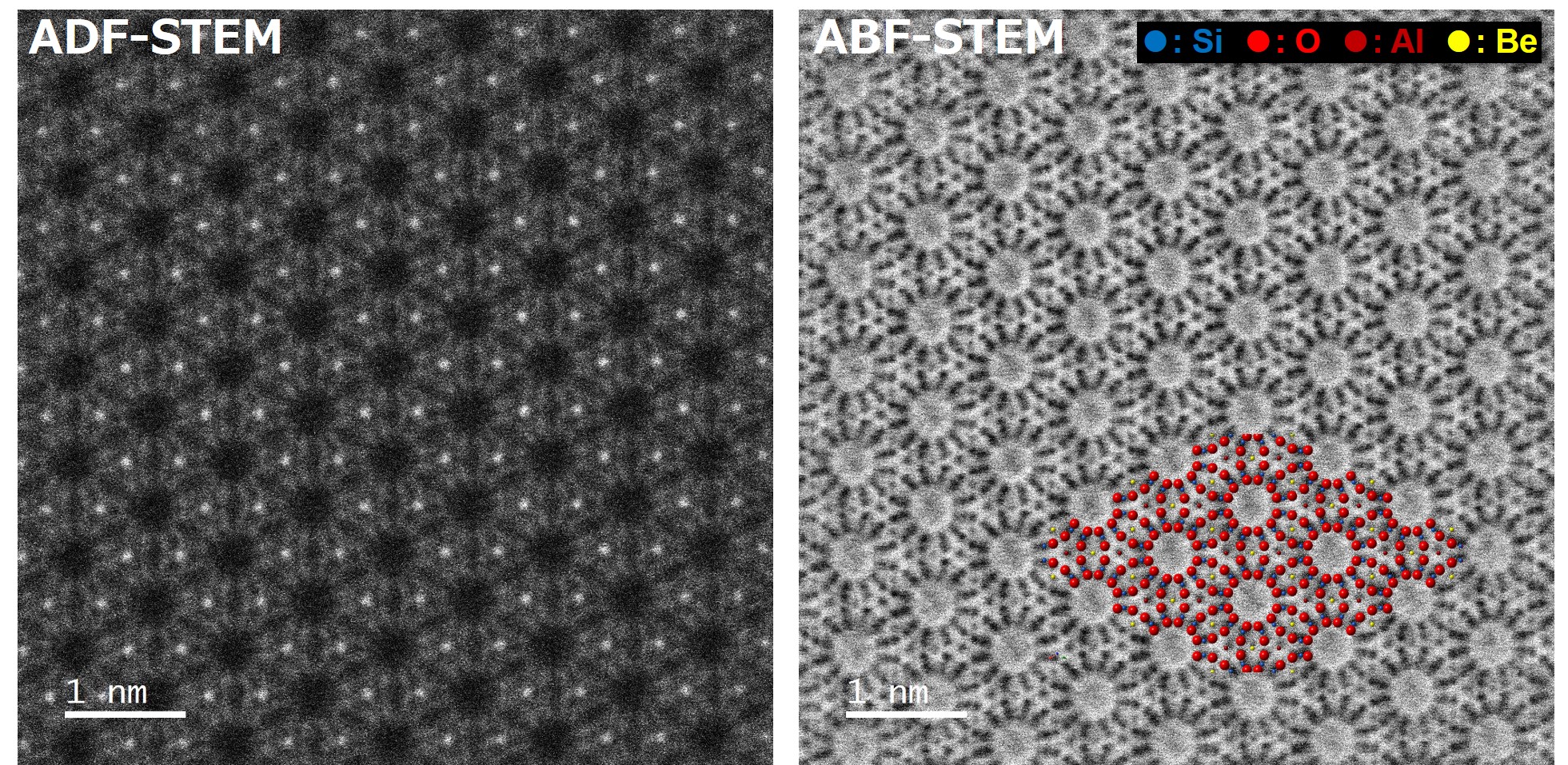
Beryl Atomic resolution STEM images STEM / Aberration correction
Glass / Ceramics, Chemistry
Atomic resolution images of Beryl [0001] obtained by using ADF-STEM and ABF-STEM methods. In the ADF-STEM method, which allows obervation of heavy elements, atomic sites of Al and Si are visible, while in the ABF-STEM method, which allows observation of light elements, Al and Si as well as O and Be are visible.
| Application | STEM / Aberration correction |
|---|---|
| Preprocessing | TEM sampling / Ar Ion milling |
| Shooting conditions | Acceleration voltage300kV、ADF & ABF STEM detectors |
| Related product | Transmission Electron Microscope (TEM) |
Related data
Are you a medical professional or personnel engaged in medical care?
No
Please be reminded that these pages are not intended to provide the general public with information about the products.