


GRAND ARM™ 3 Atomic Resolution Analytical Microscope
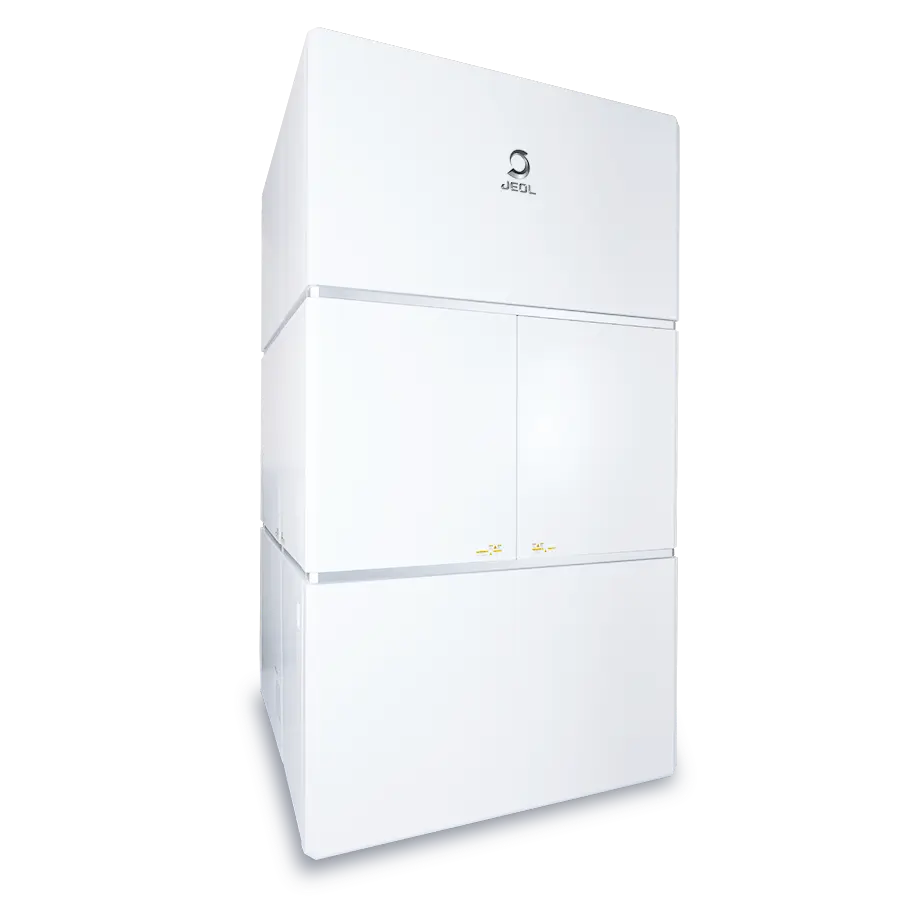
The Flagship Evolves Further.
GRAND ARM™ 3: A 300 kV TEM
Opening New Frontiers in Observation and Analysis.
JEOL's joint development with CEOS GmbH, Germany has enabled the latest aberration correctors, Large Aperture STEM Corrector (LASCOR) and Advanced TEM Corrector (ATCOR) to be installed in GRAND ARM™ 3. It realizes observation and analysis under larger aperture angles than conventional models. As a result, unprecedented ultra-high resolution observation and analysis are possible in both STEM and TEM modes.
In addition, the integration of a new high-speed scan system into GRAND ARM™ 3 enables the acquisition of STEM images of at least 30 frames per second. In-situ atomic-level observation and analysis of dynamic phenomena, which were previously difficult to study using STEM, open up new possibilities for materials research.
Features
LASCOR (Large Aperture STEM CORrector)
LASCOR, the STEM aberration corrector, uses a three-stage hexapole aberration-correction electron optical system to significantly expand the aberration-corrected area on Ronchigram in STEM mode. This makes it possible to perform observations at large convergence semi-angles and obtain high-resolution STEM images with reduced diffraction limits. In addition, as the focal depth becomes shallower as the convergence semi-angle expands, it is possible to perform depth profiling of the specimen with high resolution by performing STEM observation while changing the focal length of the objective lens in minute increments.
Performance
• HAADF-STEM resolution:
49 pm or less at 300 kV
76 pm or less at 80 kV
• Aberration correction angle range:
semi-angle of 85 mrad or more at 300 kV
Uniformed phase area in Ronchigram
(comparison with the conventional corrector
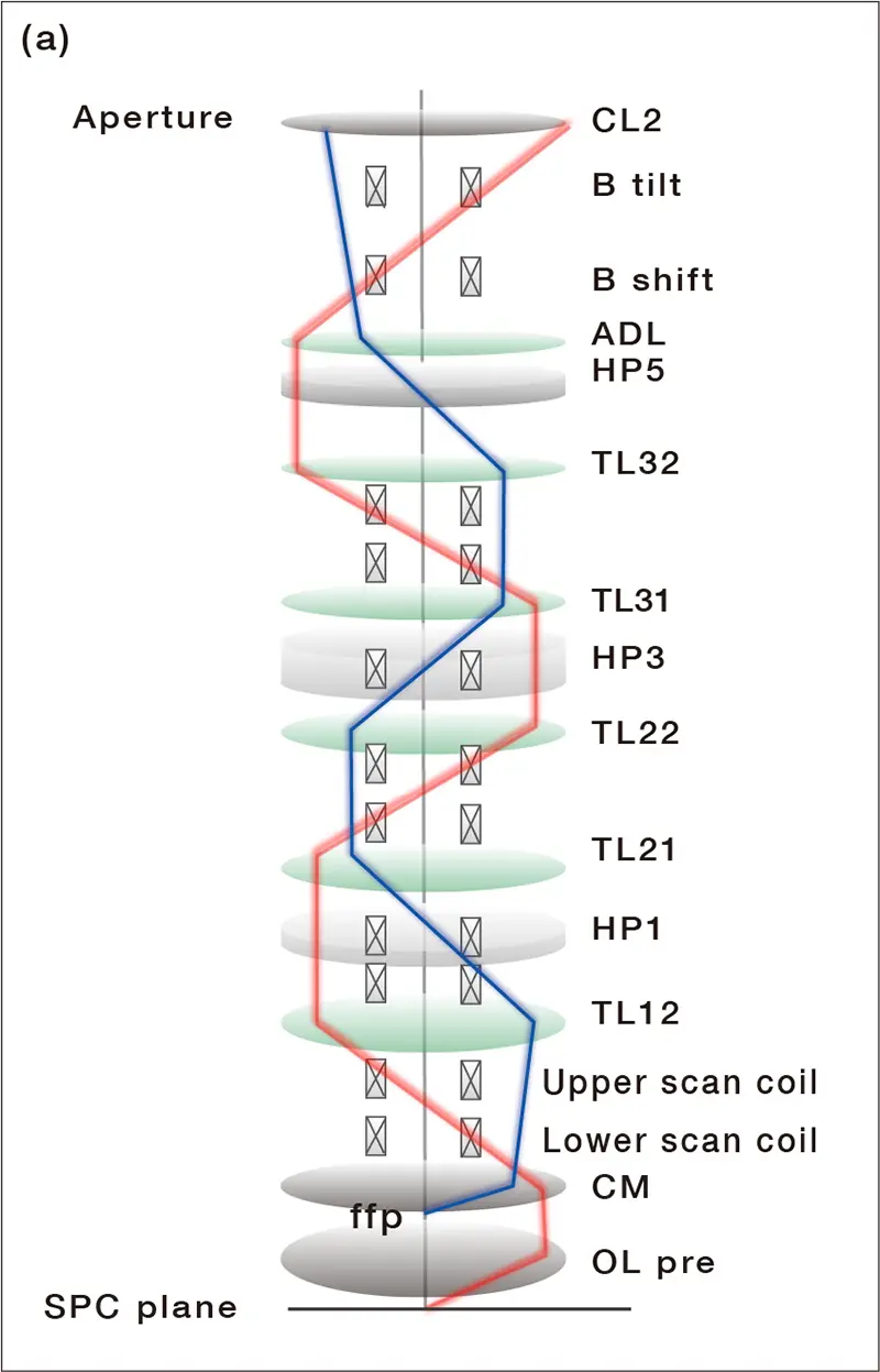
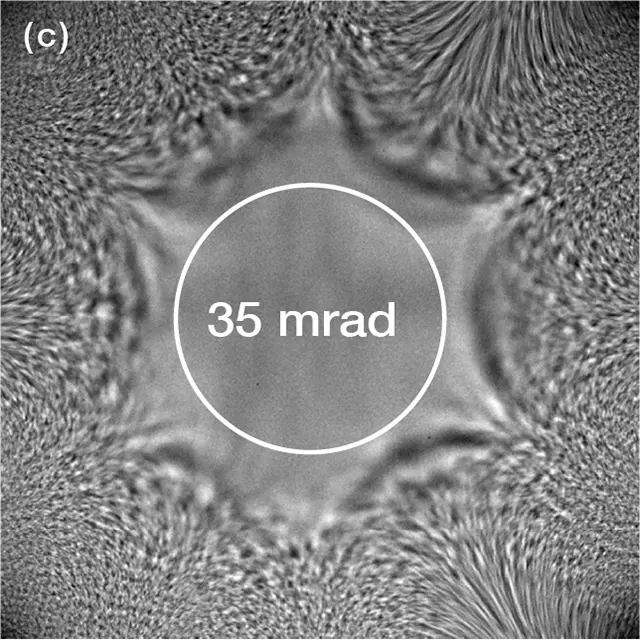
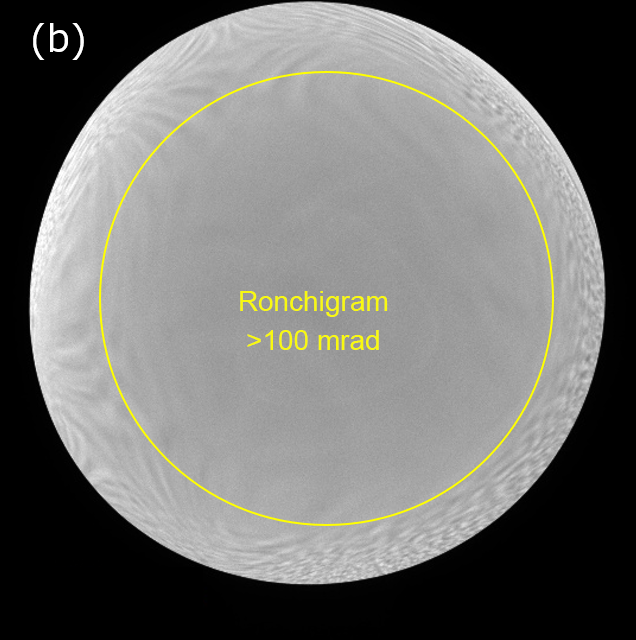
LASCOR can correct sixth-order three-lobe aberration (D6) in addition to six-fold astigmatism (A5), which is difficult to correct with conventional aberration correctors. This extends the angular space with the aberration corrected in a ronchigram in STEM mode, from the conventional 35 mrad to 85 mrad or more.
- (a) Optical arrangement and ray diagram of LASCOR
- (b) Ronchigram with an acceleration voltage of 300 kV acquired with LASCOR
- (c) Ronchigram with an accelerating voltage of 300 kV acquired with a conventional two-stage hexapole aberration corrector
High-resolution STEM image
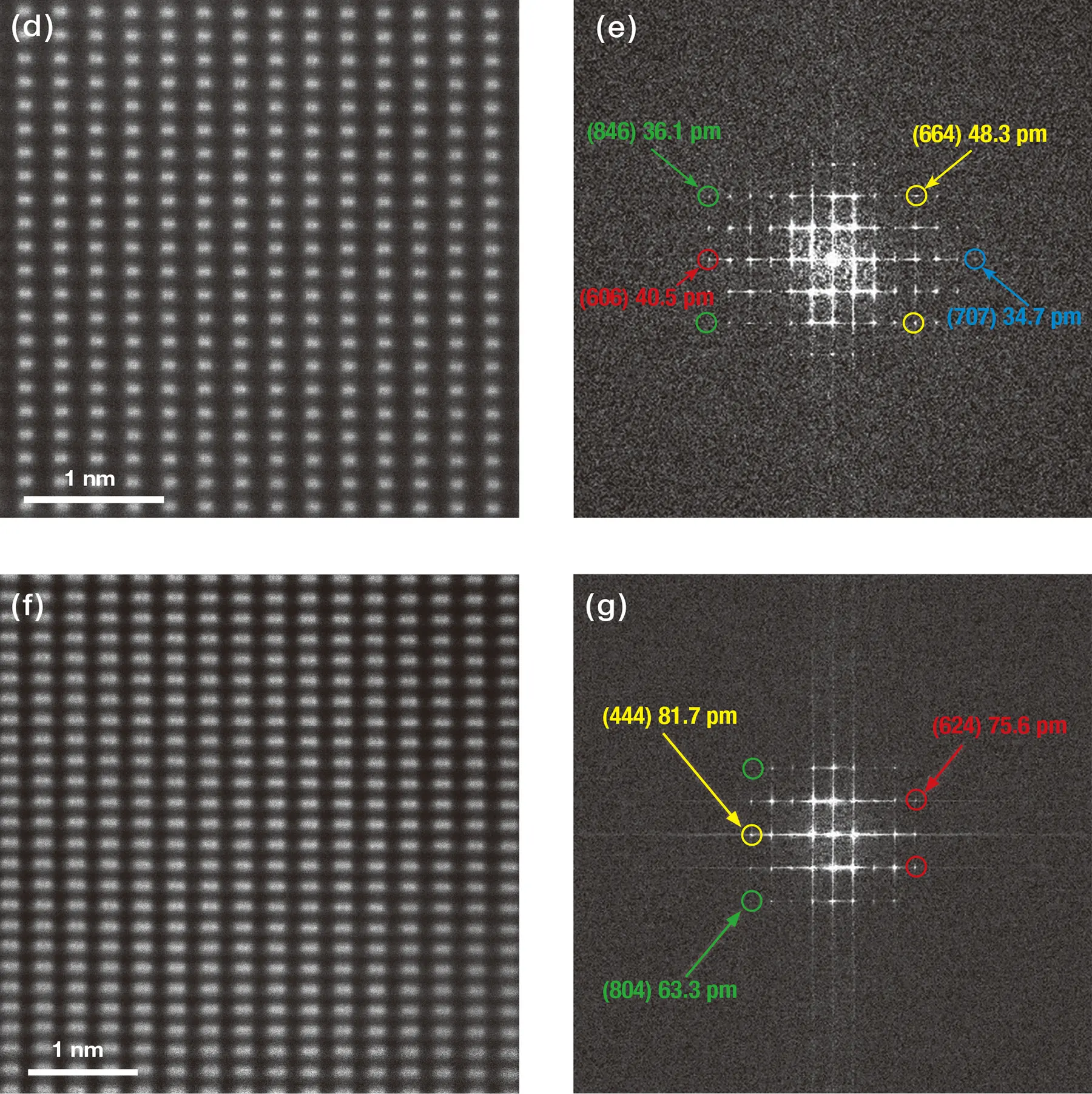
The evaluation result of HAADF-STEM resolution at acceleration voltages 300 kV and 80 kV are shown below. The reflection spots corresponding to 48.3 pm at 300 kV and 76 pm at 80 kV respectively are clearly visible. These results show that this instrument has excellent spatial resolution over a wide operating range from low to high acceleration voltages.
- (d) HAADF-STEM image of GaN [212] single crystal acquired at an accelerating voltage of 300 kV
(beam current: 23 pA, convergence semi-angle: 46 mrad) - (e) Calculated power spectra of the STEM image (d)
- (f) HAADF-STEM image of Ge [112] single crystal acquired at an accelerating voltage of 80 kV
(beam current: 23 pA, convergence semi-angle: 46 mrad) - (g) Calculated power spectra of the STEM image (f)
ATCOR (Advanced TEM CORrector)
The ATCOR (Advanced TEM Corrector) utilizes an optimized, two-stage hexapole aberration-correction electron optical system to correct six-fold astigmatism (A5), which was previously uncorrectable with conventional TEM aberration correctors. This allows electrons scattered at wider angles to contribute to imaging without being affected by aberration, improving the resolution in TEM mode. In diffraction mode, the effect of aberration on electrons scattered at wide angles is reduced, so it is possible to obtain diffraction figures with suppressed distortion.
Performance
• Lattice resolution: 50 pm or less at 300 kV
• Information limit: 60 pm or less at 300 kV
Reduction of six-fold astigmatism
(Comparison with traditional aberration corrector using diffractogram tableau)
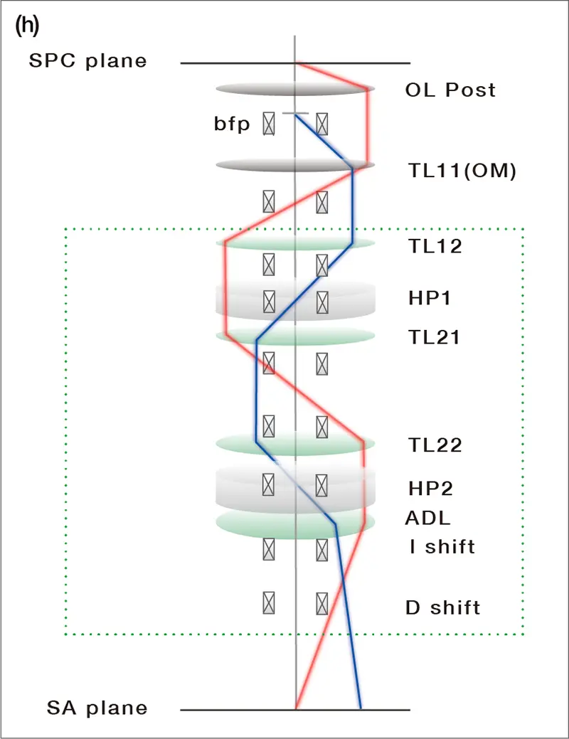
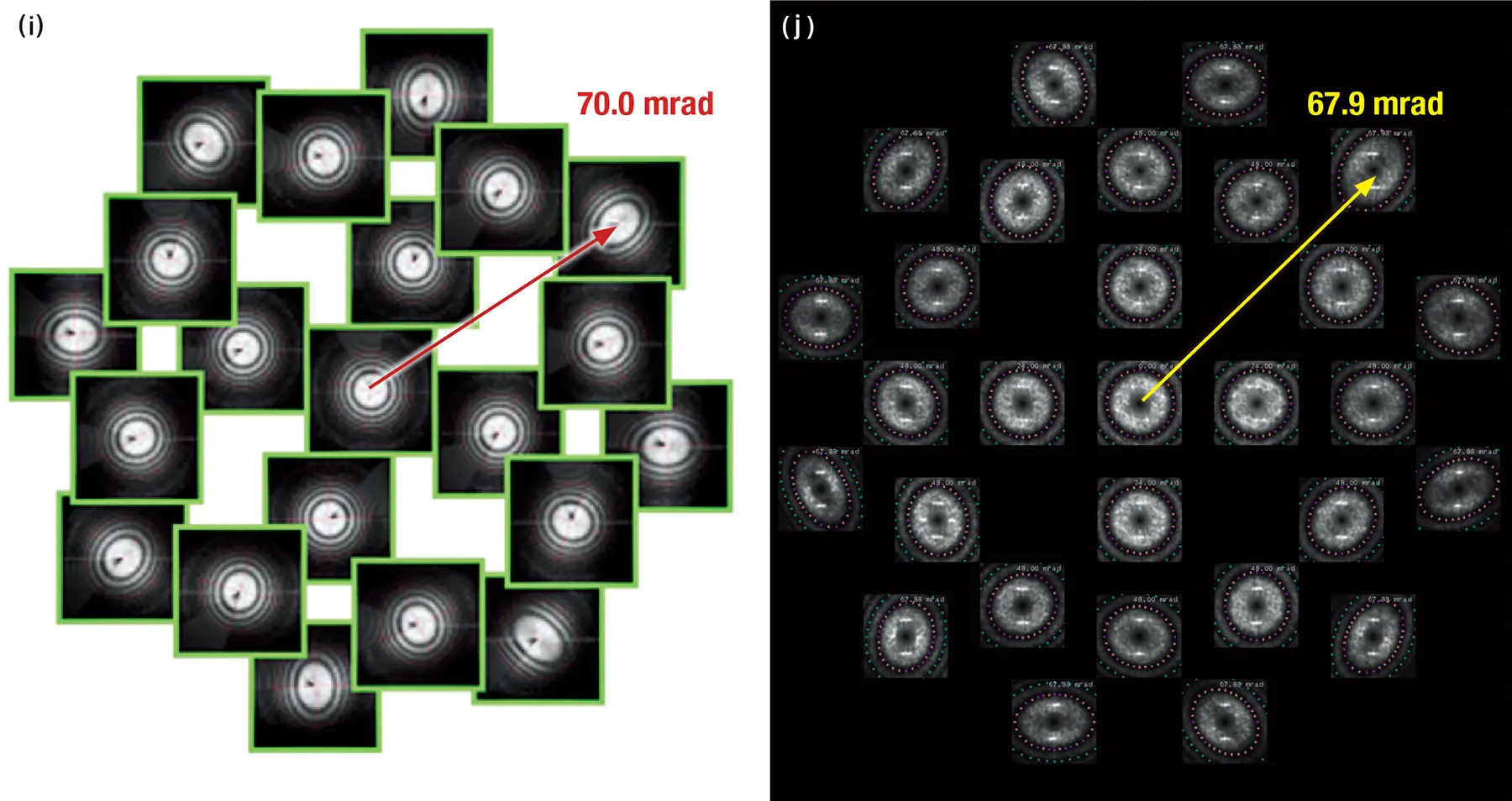
ATCOR can correct up to fifth-order aberration. From the phase rotation of the two-fold astigmatism observed in each diffractogram acquired with an incident beam tilt exceeding 60 mrad, it can be confirmed that the six-fold astigmatism (A5) is significantly reduced with ATCOR.
- (h) Optical arrangement and ray diagram of ATCOR
- (i) Diffractogram tableau with an acceleration voltage of 300 kV and a tilt angle of 70 mrad acquired with ATCOR
- (j) Diffractogram tableau with an acceleration voltage of 300 kV and a tilt angle of 67.9 mrad acquired with a conventional TEM aberration corrector
High-resolution TEM image (information limit)
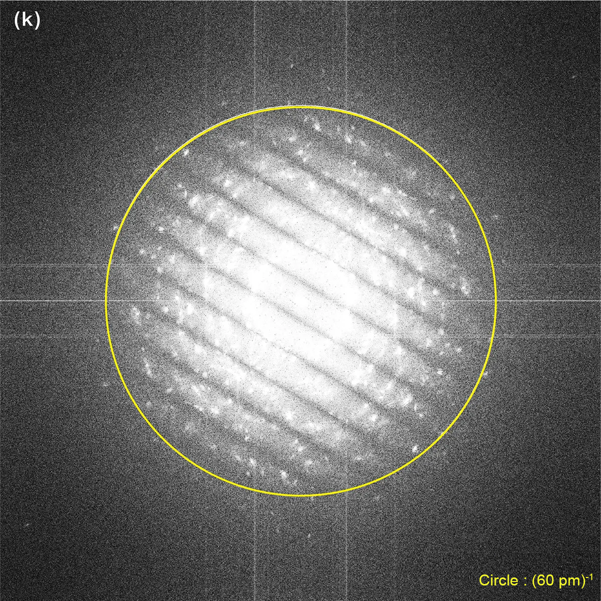
Young's fringe patterns calculated from images of a thick amorphous carbon film decorated with gold particles recorded at an accelerating voltage of 300 kV is shown below. The elongation of the fringe pattern indicates that spatial frequencies corresponding to real-space resolutions below 60 pm are transferred, demonstrating the high spatial resolution capability of the instrument.
- (k) The information limit measurement result using the Young’s fringe method for a thick amorphous carbon film decorated with gold particles acquired at an acceleration voltage of 300 kV
High-resolution TEM image (lattice resolution)
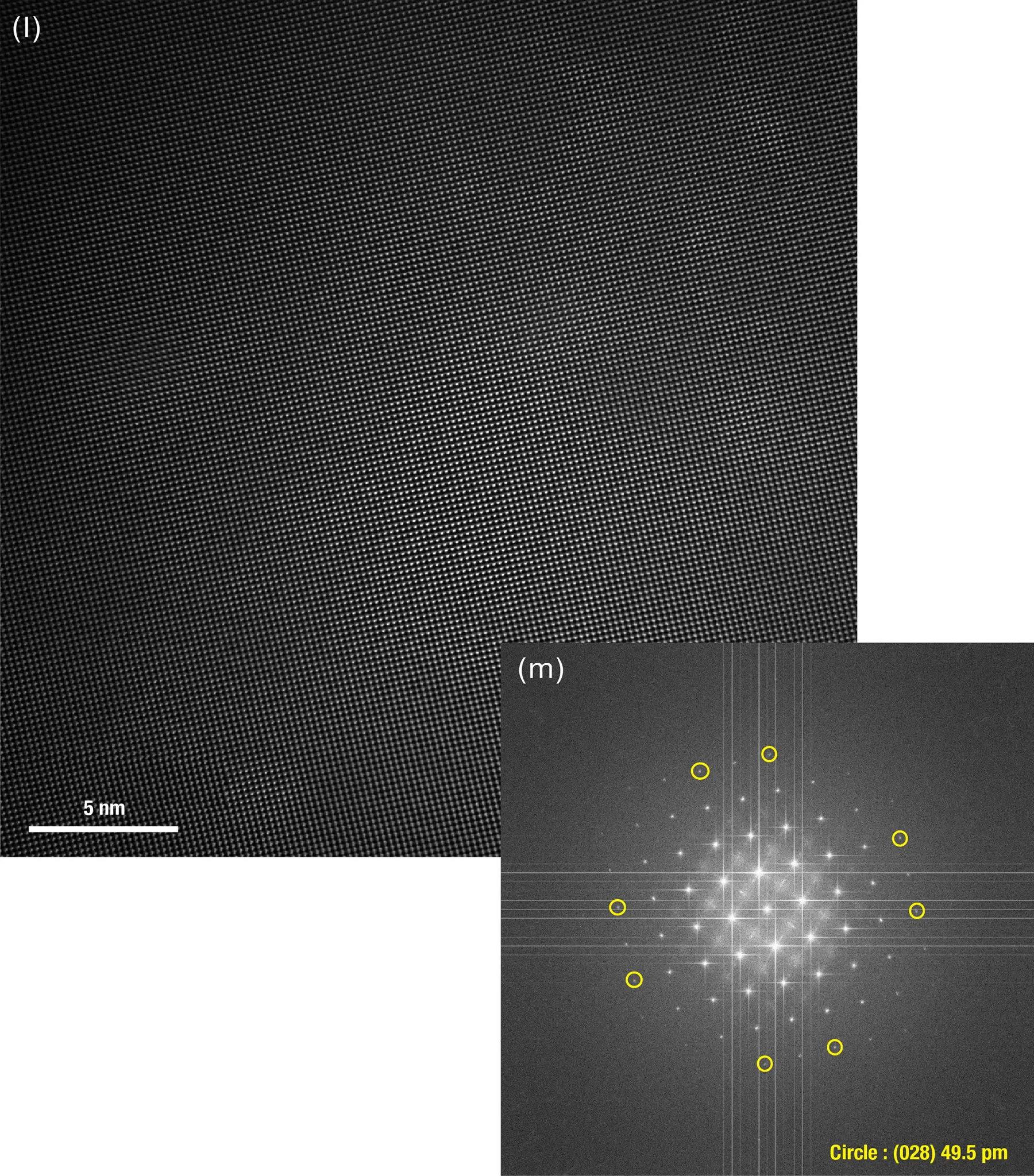
The TEM image of Au in the [100] orientation acquired at 300 kV acceleration voltage and the FFT power spectra are shown. By using ATCOR, the reflection spots corresponding to 50 pm are clearly observed, demonstrating the high stability of this instrument.
- (I) TEM image of Au [100] single crystal acquired at an acceleration voltage of 300 kV
- (m) Calculated power spectra of the TEM image (I)
EDS analysis at ultra-high resolution and sensitivity
With conventional electron microscopes, high-resolution probes can reduce the probe diameter down to the atomic scale, but the low probe current reduces the intensity of X-rays emitted from the specimen. For this reason, EDS analysis requires the use of analysis probes that prioritize probe current, creating a trade-off with spatial resolution.
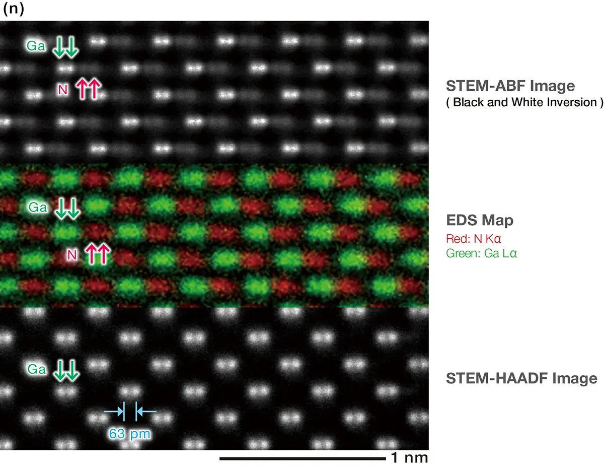
LASCOR allows us to select larger convergence angles to realize electron probes with both high probe current and high atomicscale resolution. In addition, the EDS analysis system with a 158 mm2 dual SDD, providing high X-ray detection efficiency, enables fast EDS analysis using high resolution observation probes.
The image below shows the ABF image, HAADF-STEM image, and EDS elemental mapping results of GaN [211] acquired at the same time using a probe for high-resolution observation. It shows that the elemental map with a high signal-to-noise ratio has been obtained by using a high-resolution probe suitable for atomic resolution observation.
High-Speed Scan System
The combination of a dedicated scan coil and a scintillator with a short attenuation time realizes STEM observation at 30 frames or more per second. It can be applied to in-situ observation at atomic resolution and enables tracking of dynamic phenomena such as chemical reactions in real time.
Performance
• Maximum scan speed: 83 ns/pixel or faster
• Minimum flyback time: 20 µs or less (at a scan speed of 83 ns/pixel)
• Frame rate*: 30 fps or higher with pixel size 512 × 512
• Number of simultaneous acquisition channels:
1
Note: Only the ADF detector (attached to the ADF2 port) configured in this product is supported.
• Maximum scan area: 400 × 400 nm or more
Faster STEM technology
With conventional technology, the acquisition of 512 × 512 pixel STEM images was limited to one to two frames per second. In contrast, the number of turns of the scan coil was reduced from that of the conventional product, and the inductance was reduced to 1/240 of that of the conventional product. This greatly reduced the flyback time from 500 µs to 20 µs or less. Furthermore, a scintillator with a shortened fluorescence life realizes a Nyquist frequency of 6 MHz. In addition to these improvements for a faster scan, a high-speed data transfer system that supports high-speed STEM observation has been developed.
Comparison with conventional STEM imaging
Comparison of this high-speed scan system with a conventional scanning system (50 times faster atomic resolution STEM movie) Specimen: SrTiO3 [100]
High-speed STEM observation video
Scan speed: 0.083 µs/pix
Flyback time: 20 µs
STEM image acquisition rate: 25 fps
Conventional STEM observation videos
Scan speed: 4 µs/pix
Flyback time: 400 µs
STEM image acquisition rate: 0.5 fps
Data provided by Dr. Ryo Ishikawa, Project Associate Professor, Institute of Engineering Innovation,
School of Engineering, the University of Tokyo
Specifications
Please refer to the catalog.
Catalogue Download
Comig soon.
Related Products
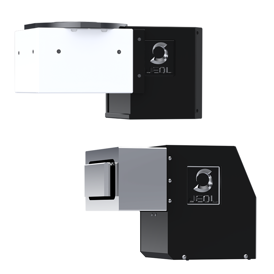
SightSKY™ Series High-Sensitivity, Low-Noise Fiber-Coupling CMOS Camera
High-sensitivity, low-noise 19 M pixel CMOS sensor enables imaging of fine specimen detail and obtains high signal to noise images even at low electron doses.A Global shutter and high frame rate (58 fps/full pixel mode) enable image series acquisitions with less artifacts during in-situ dynamic observation studies.The SightSKY™ camera system offers integration with JEOL’s FEMTUS™ Integrated Analysis Platform, providing user-friendly operation and data acquisition.
More Info


Are you a medical professional or personnel engaged in medical care?
No
Please be reminded that these pages are not intended to provide the general public with information about the products.