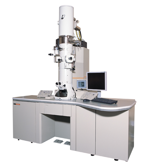
【DISCONTINUED】JEM-2100F Field Emission Electron Microscope
DISCONTINUED
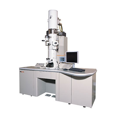
This product is no longer available.
If you would like to know the latest information about your preferred product or to find out more about alternatives, please click on the link below. We hope you will continue to use our products.
The JEM-2100F is a multipurpose, 200 kV FE (Field Emission) analytical electron microscope. Variety of versions is provided to adapt user’s purposes. The FE electron gun (FEG) produces highly stable and bright electron probe that is never achieved with conventional thermionic electron gun. This feature is essential for ultrahigh resolution in scanning transmission microscopy and in an analysis of a nano-scaled sample. Various analytical instruments and/or cameras such as EDS (Energy Dispersive X-ray Spectrometer) or EELS (electron energy loss spectrometer) or CCD cameras are ready for integration with a PC system of the microscope control.
Features
FETEM, for high resolution observation and nano scale analysis
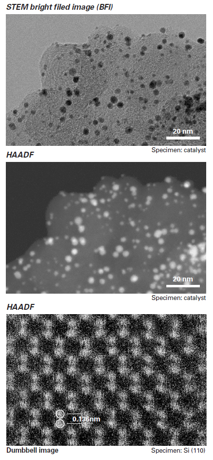
FEG featuring a high brightness and a high stability realizes structural scanning imaging at atomic resolution. Highly bright sub-nanometer sized probe enables us to perform an ultimately sensitive analysis of a sample at sub-nanometer resolution. With FEG, the contrast of high-resolution image is also improved because it provides a highly coherent illumination with a narrow energy spread. In addition, the electron holography that requires the highly coherent illumination is available for this microscope with an optional equipment electron bi-prism.
Highly stable specimen driving system
The stable specimen driving system enables us to perform analysis at nanometer scale. The system allows the specimen to perform tilt and/or shift with an ultra low drift and vibration. With optionally available piezo specimen drive system, specimen can be shifted at sub-nanometer resolution with a range of ± 1.2 μm.
Since, the system accepts variety of specimen holders, various physical conditions of specimen such as temperature or rotation or tilt can be changeable.
Integration to other instruments
The microscope can be fully controlled by PC. The design concept enables us to integrate various analytical instruments and/or cameras such as EDS or EELS or CCD cameras.
Specifications
| Configuration※1 | Ultrahigh resolution (UHR) |
High resolution (HR) |
High specimen tilt (HT) |
Cryo polepiece (CR) |
High contrast (HC) |
|---|---|---|---|---|---|
| Polepiece | URP | HRP | HTP | CRP | HCP |
| Resolution | |||||
| Point | 0.19 nm | 0.23 nm | 0.25 nm | 0.27 nm | 0.31 nm |
| Lattice | 0.1 nm | 0.1 nm | 0.1 nm | 0.14 nm | 0.14 nm |
| Acc. Voltage※2 | 160 kV,200 kV※1 | ||||
| Minimum step | 50 V | ||||
| Step size | 50 V minimum | ||||
| Electron source | |||||
| Emitter | ZrO/W(100) Schottky | ||||
| Brightness | ≧4×10⁸ A / cm2 / sr | ||||
| Pressure | ×10-8 Pa order | ||||
| Probe current | 0.5 nA for 1 nm probe | ||||
| Power Stability | |||||
| Acc. voltage | ≦1×10⁻⁶/min | ||||
| OL current | ≦1×10⁻⁶/min | ||||
| Optical parameters for objective lenses | |||||
| Focal length | 1.9 mm | 2.3 mm | 2.7 mm | 2.8 mm | 3.9 mm |
| Spherical aber. coef. | 0.5 mm | 1.0 mm | 1.4 mm | 2.0 mm | 3.3 mm |
| Chromatic aber. coef. | 1.1 mm | 1.4 mm | 1.8 mm | 2.1 mm | 3.0 mm |
| Minimum focal step | 1.0 nm | 1.4 nm | 1.8 nm | 2.0 nm | 5.2 nm |
| Spot Size (diameter) | |||||
| TEM mode | 2 to 5 nm | 7 to 30 nm | |||
| EDS mode | 0.5 to 2.4 nm | - | - | 4 to 20 nm | |
| NBD mode | - | - | - | ||
| CBD mode | 1.0 to 2.4 nm | - | |||
| Parameters for convergent beam diffraction | |||||
| Convergence angle | 1.5 to 20 mrad | - | - | ||
| Acceptance angle | ±10° | - | - | ||
| Magnification | |||||
| MAG mode | ×2,000 to 1,500,000 | ×1,500 to 1,200,000 | ×1,200 to 1,000,000 | ×1,000 to 800,000 | |
| LOW MAG mode | ×50 to 6,000 | ×50 to 2,000 | |||
| SA MAG mode | ×8,000 to 800,000 | ×6,000 to 600,000 | ×5,000 to 600,000 | ×5,000 to 400,000 | |
| Camera Length | |||||
| SA diffraction(mm) | 80 to 2,000 | 100 to 2,500 | 150 to 3,000 | ||
| HD diffraction(m) | 4 to 80 | ||||
| HR diffraction※2 | 333 mm | ||||
| Specimen shift | |||||
| X,Y | 2 mm | 2 mm | 2 mm | 2 mm | 2 mm |
| Z | ±0.1 mm | ±0.2 mm | ±0.2 mm | ||
| Specimen tilt | |||||
| X/Y※3 | ±25/±25° | ±35/±30° | ±42/±30° | ±15/±10° | ±38/±30° |
| X※4 | ±25° | ±80° | ±80° | ±80° | ±80° |
| STEM※5 | |||||
| Bright-field lattice resolution | 0.2 nm | - | - | ||
| EDS※6 | |||||
| Solid angle(30mm2) | 0.13 sr. | 0.13 sr. | 0.13 sr. | ※8 | 0.09 sr |
| Solid angle(50mm2)※7 | 0.24 sr. | 0.28 sr. | 0.23 sr. | ||
| Take-off angle(30mm2) | 25° | 25° | 25° | ※8 | 20° |
| Take-off angle(50mm2)※7 | 22.3° | 24.1° | 25° | ||
Select either configuration when ordering the JEM-2100F.
80 kV, 100 kV and 120 kV are possible with the optional short-circuit switches for the accelerating tube.
With the Specimen Tilting Holder (EM-31630).
With the High Tilt Specimen Retainer (EM-21310).
With the optional scanning image observation device.
With the optional EDS detector.
With the JEOL 50 mm2 EDS detector.
EDS detectors are unavailable.
Application
Application JEM-2100F
Adapting a JEM-2100F for Magnetic Imaging by Lorentz TEM
Gallery
-

-
-
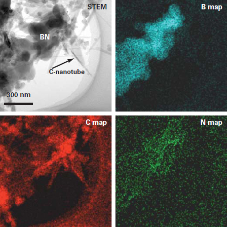
Specimen: Carbon Nanotube on Boron Nitride
Specimen Courtesy of Dr.Yoshio Baondo, International Center for Materials Nanoarchitectonics, National Institute of Material Science -
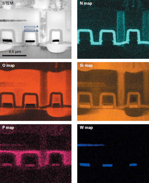
Specimen: DRAM
Related Products
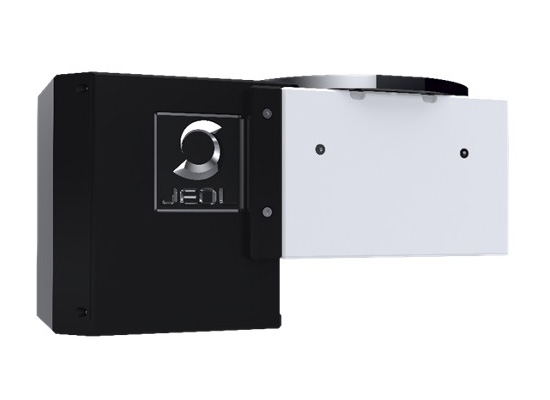
SightSKY Camera (EM-04500SKY) High sensitivity, Low noise fiber coupling CMOS camera
High-sensitivity, low-noise 19 M pixel CMOS sensor enables clearer imaging with fine specimen details observable even at low electron doses.
Its global shutter and high frame rate (58 fps/full pixel mode) enable image series acquisitions with less artifacts during dynamic observation.
"SightX" camera system control software provides user-friendly operations.
More Info
Are you a medical professional or personnel engaged in medical care?
No
Please be reminded that these pages are not intended to provide the general public with information about the products.
