


JCM-7000Plus
NeoScope™ Benchtop SEM
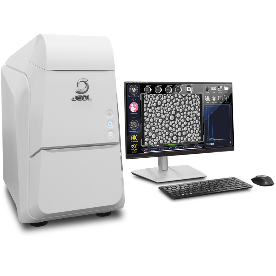
Observe "Now". Act "Next"
Live Observation, Evolved. Benchtop SEM
The JCM-7000Plus benchtop SEM transforms a routine observation into immediate insight. By combining high-quality SEM imaging with real-time elemental analysis and automated workflows, this benchtop SEM helps users quickly understand their specimens and move confidently to the next step.
Whether screening materials, investigating defects, or performing quality control, the JCM-7000Plus delivers the information you need—when you need it.

Features
Observe "Now"
From a Simple SEM observation to Live analysis
Act "Next"
High-quality data to support your decision
Zeromag
Seamless operation from optical to SEM imaging
Zooming in on the optical image automatically switches to an SEM image.
・Viewing is simple with no pre-treatment needed in a standard low vacuum mode.
・Furthermore, the JCM-7000Plus automatically adjusts the contrast and brightness, focus, and astigmatism to quickly produce high-quality SEM images
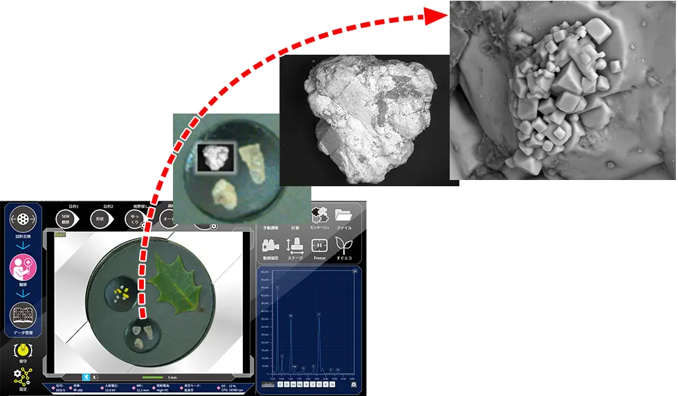
Specimen: Salt
Specimens: Tablet and Shark Tooth
Advanced four Live functions
Gain immediate understanding of your specimen while you observe
01. Live Analysis
Elemental analysis during observation
JEOL is one of the few manufacturers that develops both electron microscopes and EDS system in-house. The x-ray spectrum of the area under observation, and the major elements identified after automatic qualifications can be displayed on the observation screen in real-time. Observation and elemental analysis can be performed on the same screen, enabling a smooth analysis without interrupting your workflow. In addition, since electron microscopes and EDS are integrated in design, automated measurement (NeoAction) can be performed.
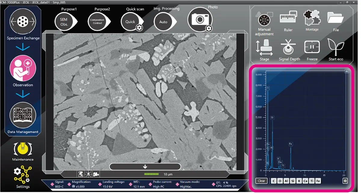
Observed image and elemental analysis on the same screen
Specimen:Alloy
02. Live Map
Visualizes elemental distribution
in real-time
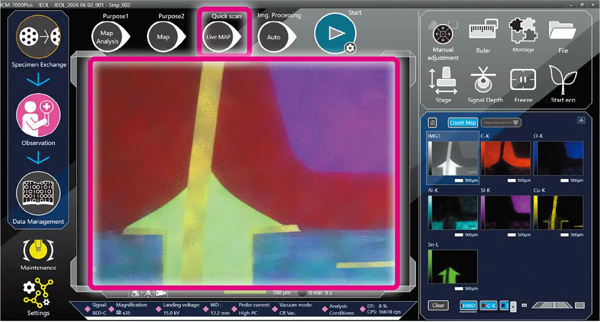
Specimen: Metal fracture surface
03. Live 3D
Instantly reveals surface topography
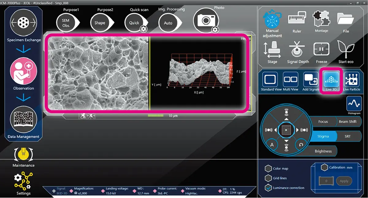
Specimen: Electronic component cross-section
04. Live Particle
Automatic measurement of particle size
Particles are automatically detected from the SEM image. Particle size distribution, average particle size, and variation can all be obtained in real time.
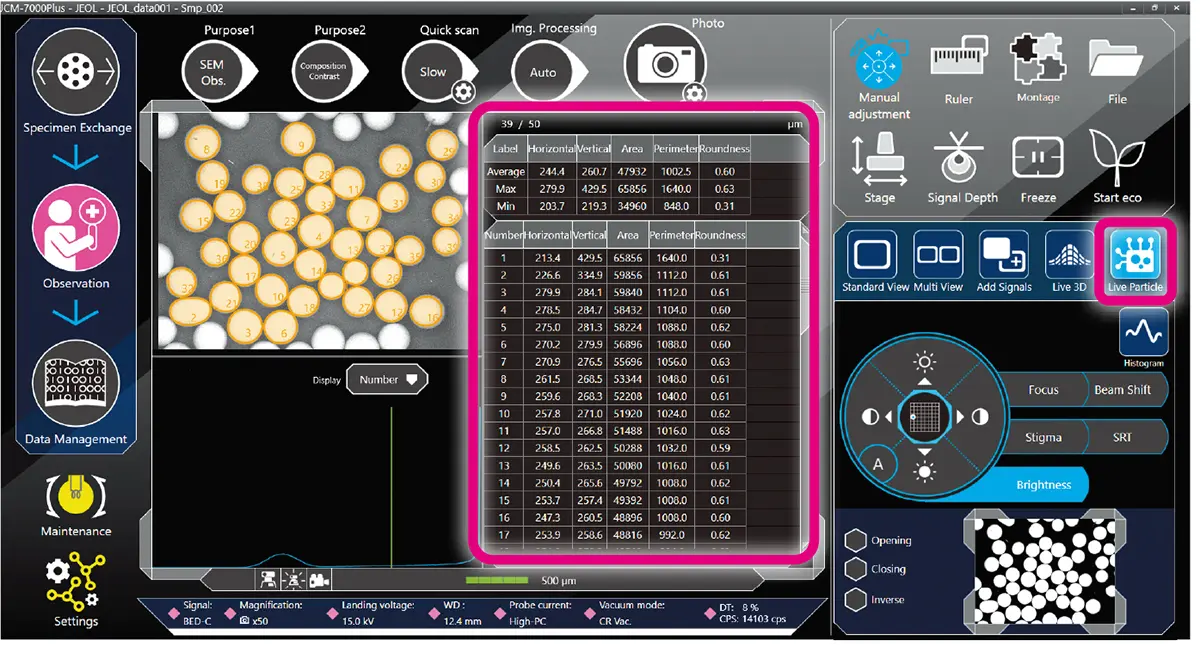
Specimen: Silicon oxides particles
Low Vacuum Mode
Observe specimens as they are with no pre-treatment
When an electron beam is irradiated onto a non-conductive (insulating) specimen, electrons accumulate on the specimen surface, causing a phenomenon known as "charging". This can result in washed-out images, distortion, and image noise. In low-vacuum mode, stable observation is possible by introducing gas or air into the specimen chamber to reduce charging. Insulating specimens such as glass and ceramics as well as moisture/easily-charged specimens such as food, polymer, and living things can be observed and analyzed with no coating needed.

Speedy observation and analysis with SEM with no specimen treatment
- Example of low vacuum mode -
Why not observe non-conductive insulating specimens in the SEM without any pretreatment? Here, we present examples of effective applications of the JCM-7000 in low vacuum (LV) mode, for polymer materials, industrial materials, minerals, food, and biological/plant specimens.
Auto Image Adjustment x High Vacuum Mode x High Resolution
6 nm resolution achieved
The JCM-7000Plus adopts landing voltage(accelerating voltage) up to 20 kV! Enhanced automatic image adjustment function and the proven high vacuum mode from the previous model improved the resolution even higher! High resolution observation and high precision EDS analysis deliver a higher level of data quality.
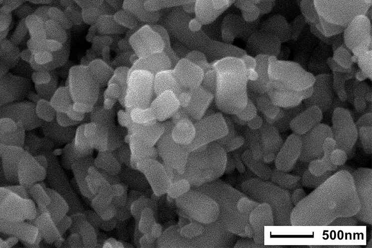
Specimen: Zinc oxide particles
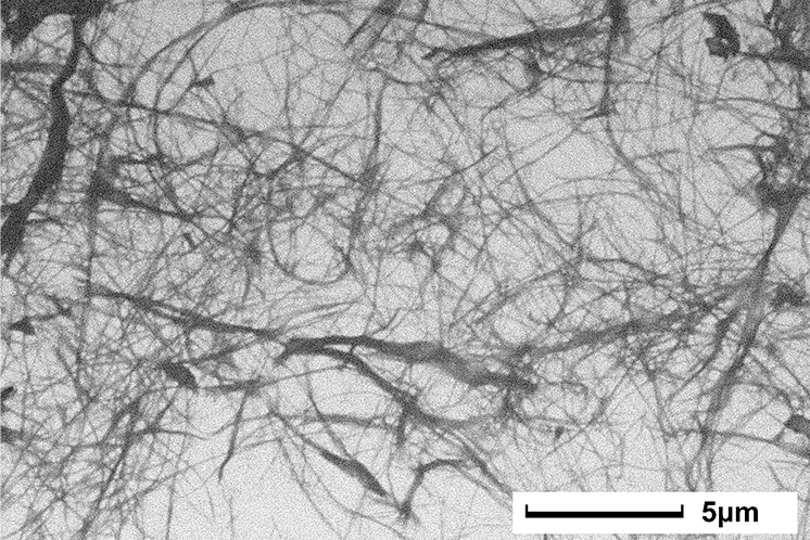
Specimen: Chitin nanofibers
(using a simplified STEM holder)
Specimen provided by OMURATORYO Co., Ltd.
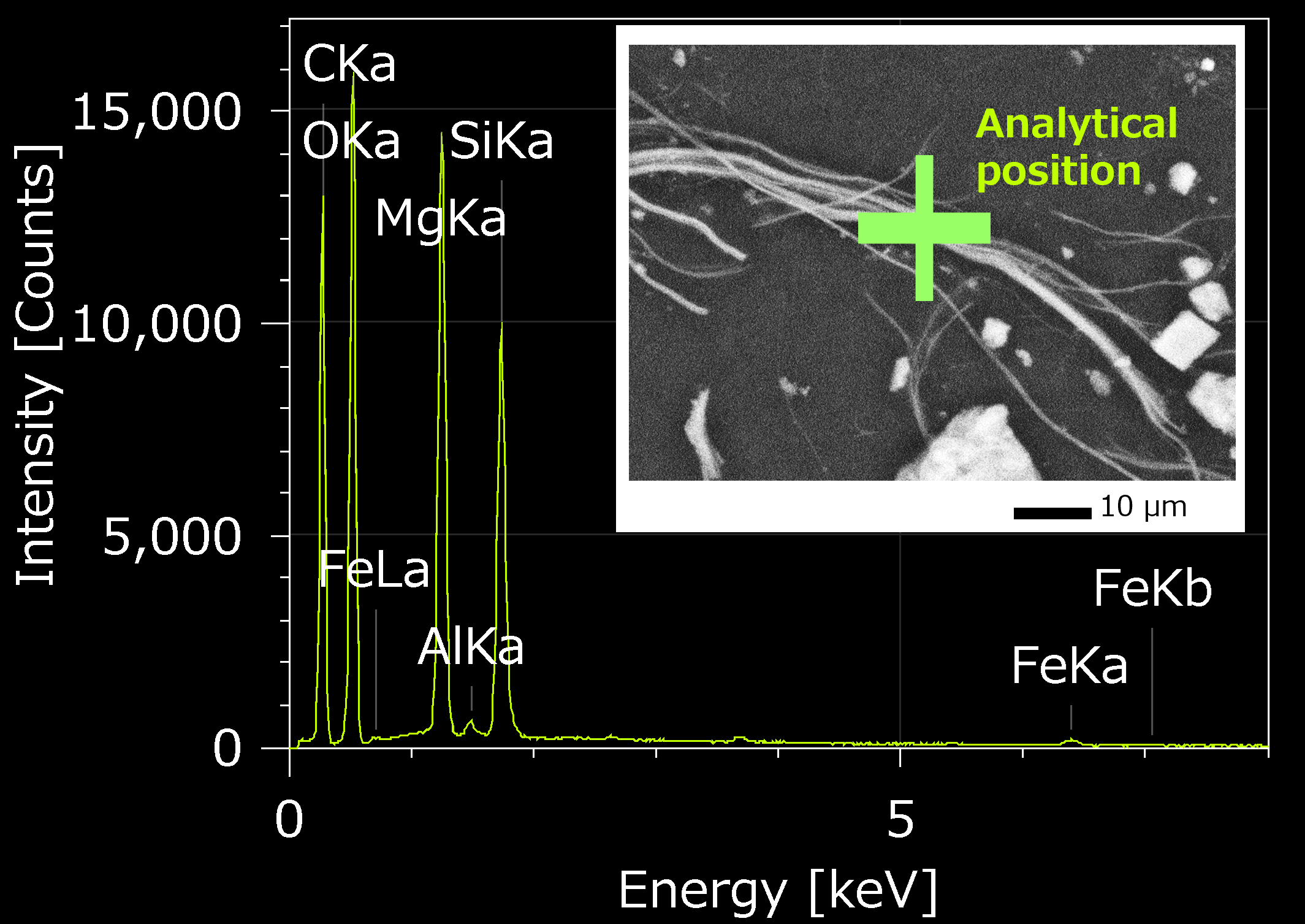
Specimen: Asbestos-containing building material
High Vacuum Mode
Highly precise observation and analysis
In high‑vacuum mode, electron scattering is minimal and secondary electrons can be detected efficiently, enabling a clear observation of microstructures at high magnifications. In addition, elemental analysis with reduced qualitative error is possible in EDS analysis. Despite being a benchtop SEM, it delivers high-precision data for both morphological observation and elemental analysis.
Enhanced automated functions
Neo Action
Automate repetitive measurements
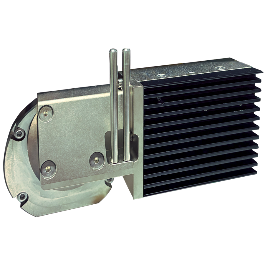
Neo Action (option) is an SEM function to automatically observe/analyze specimen by changing conditions such as landing voltage/signals, automatic image adjusting, and changing positions based on predefined workflows, as if operated by an operator.
This allows for unattended routine work from data acquisition to report generation.
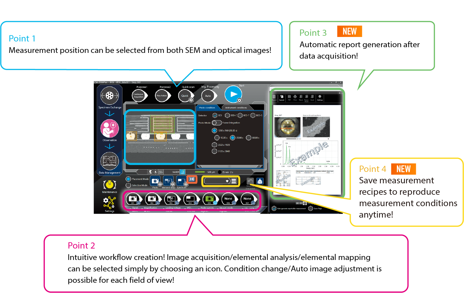
Montage
Automatic acquisition of data from a wide area
It is a function that automatically acquires a specified millimeter‑scale wide area.
The SEM automatically moves the stage and captures images, then stitches the acquired SEM images to generate a wide‑area image or mapping.
Because it can obtain high‑pixel images over a large field of view, it enables analysis from the overall structure down to localized regions, and provides data that can be easily-understood even by users who did not perform the measurement.
Multiple Field of View Analysis
Automatic measurement of multiple field
Automatic measurement of multiple locations is possible even with different fields of view, simply by specifying the acquisition condition and area of analysis. High precision stage control enables stable data acquisition.
Specifications
Main specifications
| Resolution | 6.0 nm (20 kV, WD 12mm, High-vacuum mode, Secondary electron image) 8.0 nm (20 kV, WD12 mm, High-vacuum mode, Backscattered electron image) |
|---|---|
| Direct magnification | ×10 to 100,000 (Magnification is defined by 128 mm × 96 mm) |
| Mode | High-Vacuum mode:Secondary electron image, Backscattered electron image (composition, topographic and shadow, 3D images) Low-Vacuum mode:Backscattered electron image (composition, topographic and shadow, 3D images) |
| Landing voltage (Accelerating voltage) |
5 kV, 10 kV, 15 kV, 20 kV (4 stages) |
| Electron source | Tungsten filament/ Wehnelt integrated grid |
| Specimen stage | X-Y motor drive stage X: 40 mm Y: 40 mm |
| Maximum specimen size | 80 mm diameter × 50 mm height |
Catalogue Download
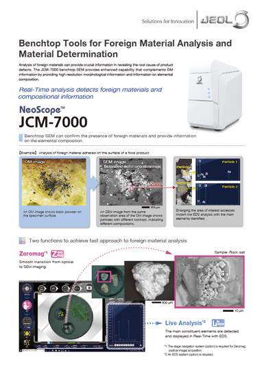
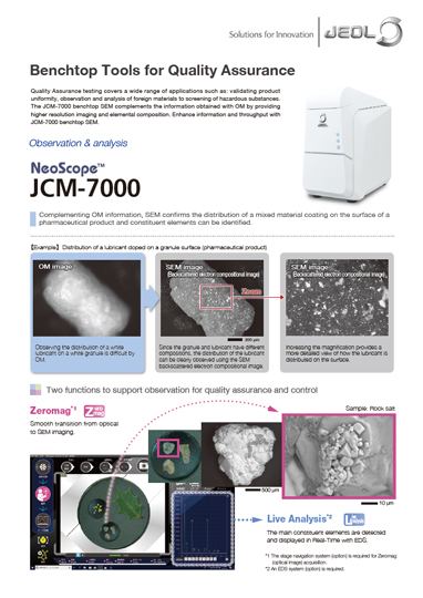
Application
Gallery
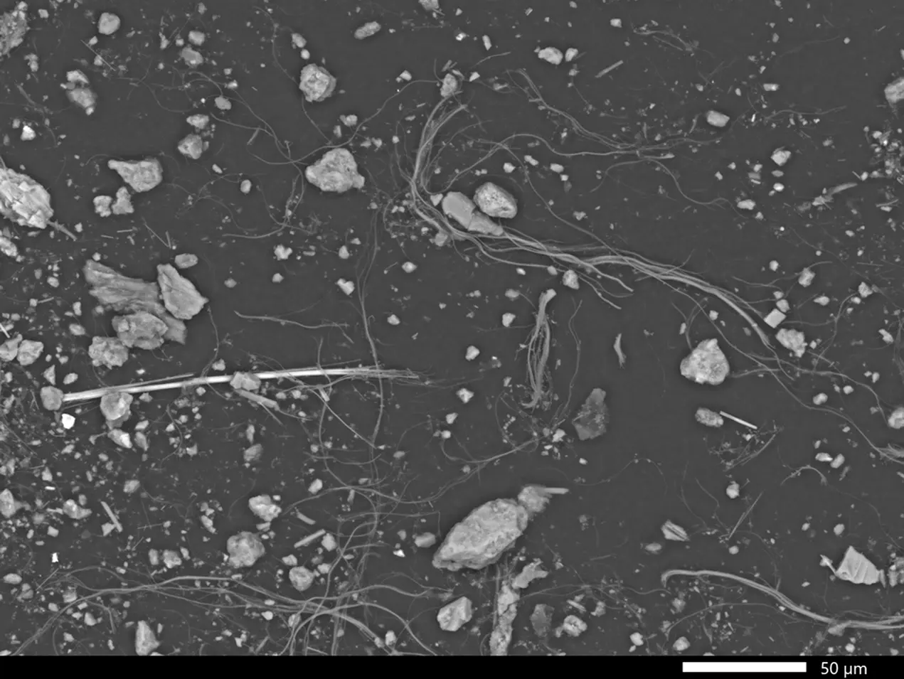
Asbestos-containing building material
Mineral Identification
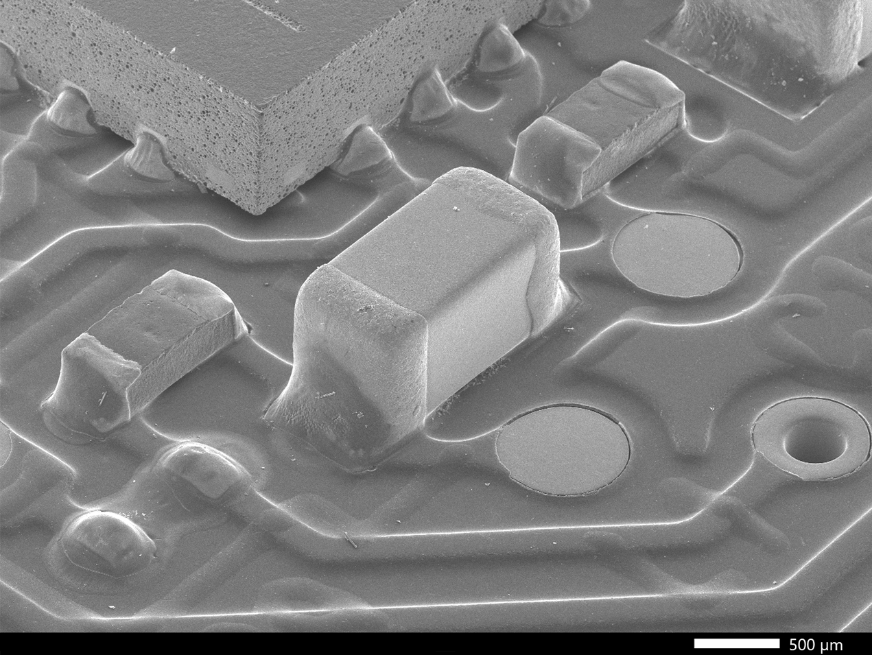
Circuit board
Failure analysis
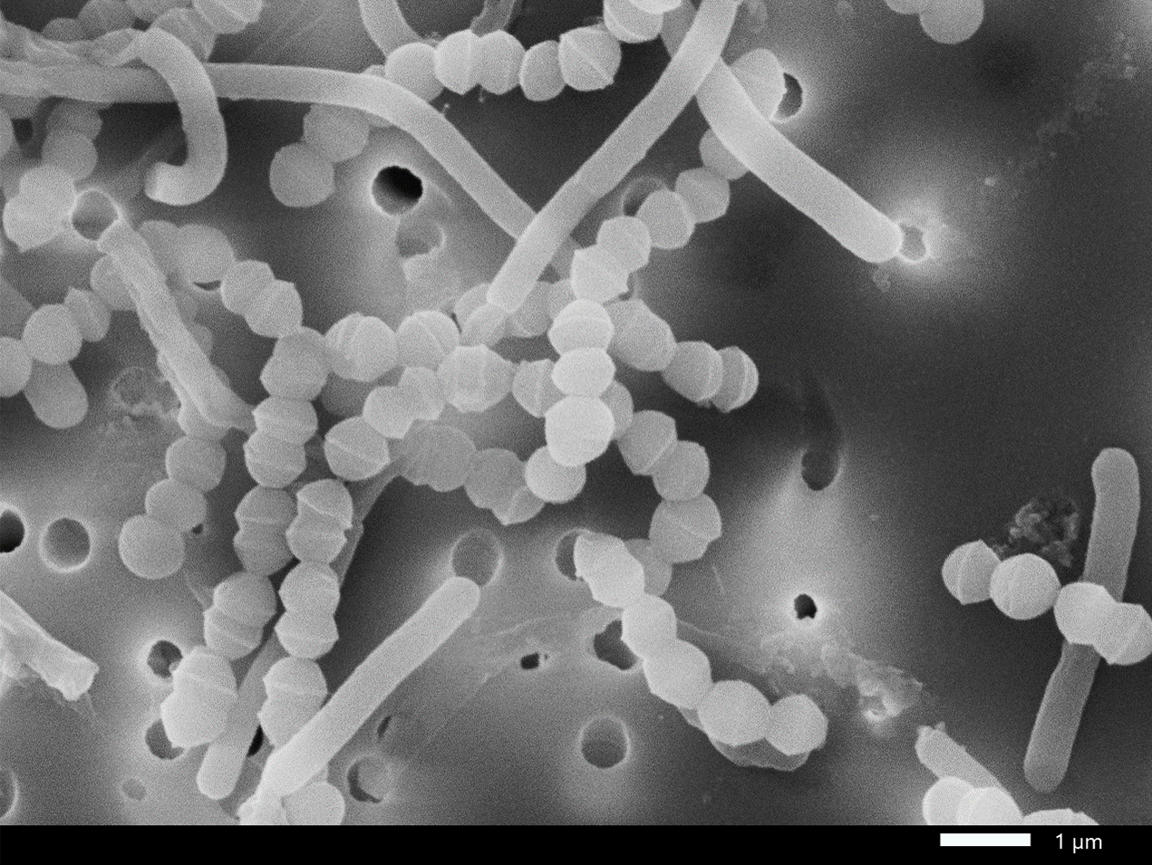
Lactic acid bacteria
Microorganism observation
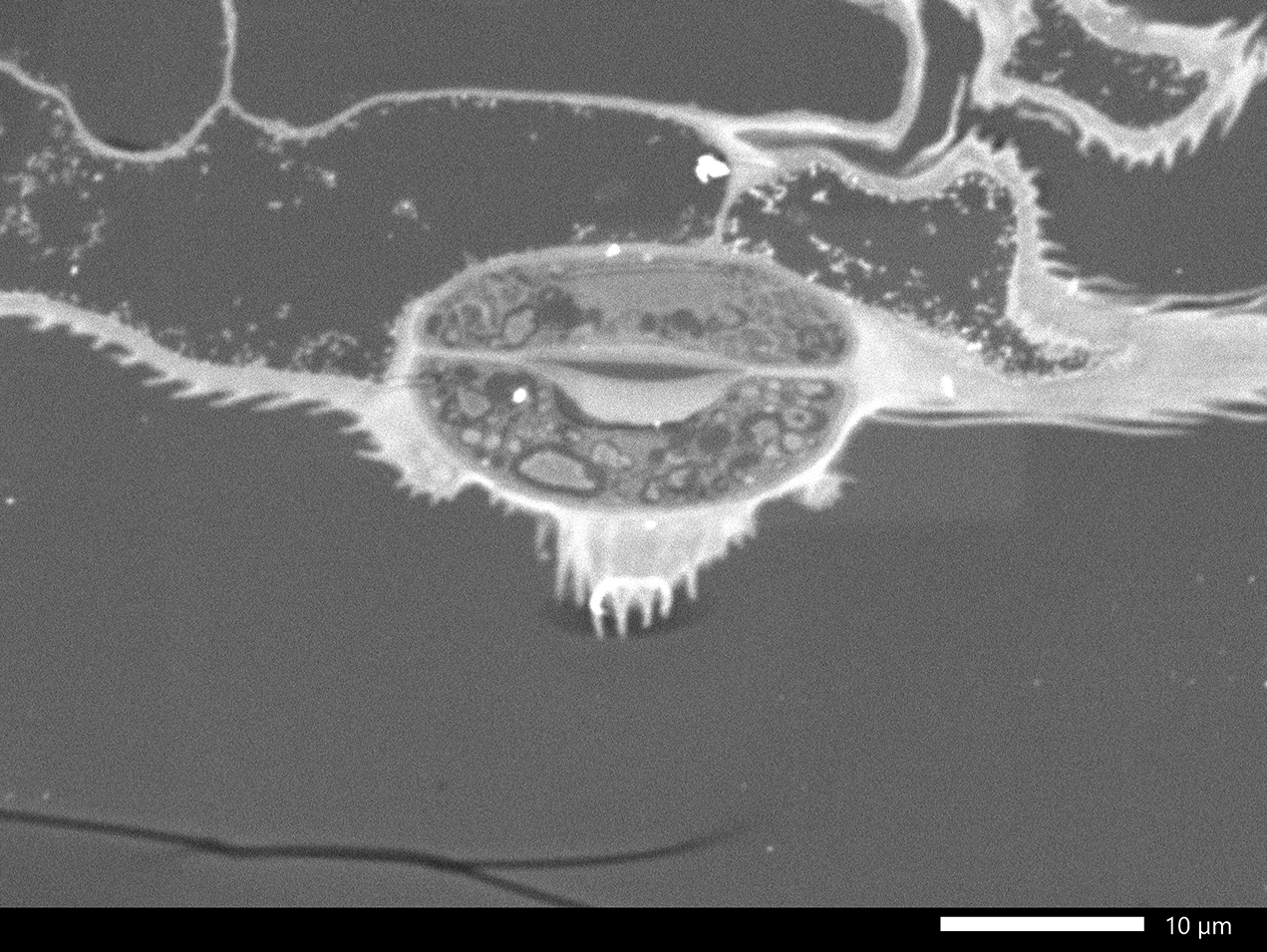
Carrot Leaf Cross Section
Internal Observation
Applications Related to the JCM-7000Plus
Cross Sections of Noodles Observed at Various Cooling Temperatures
More Info
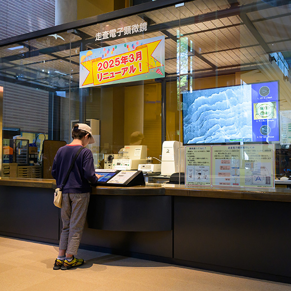
【Selected list of installations】Ibaraki Nature Museum
Ibaraki Nature Museum (Bando, Ibaraki prefecture) introduced a benchtop scanning electron microscope (SEM) which can be operated by visitors. All operations necessary for observations are performed through a touch panel. It will provide an appealing new exhibition that will make children "want to go there again".
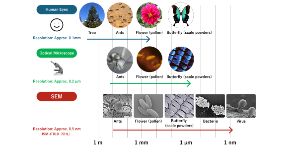
Differences between Electron Microscopes (SEM/TEM) and Optical Microscopes (OM) - Mechanism, Features, and Observation Examples
A microstructure that is not visible with our naked eyes can be observed in detail when a microscope is used. The figure below illustrates the differences in observable size and resolution among the "human eyes", "Optical Microscopes", and "Electron Microscopes (SEM)"


Are you a medical professional or personnel engaged in medical care?
No
Please be reminded that these pages are not intended to provide the general public with information about the products.