


Differences between Electron Microscopes (SEM/TEM) and Optical Microscopes (OM) - Mechanism, Features, and Observation Examples
A microstructure that is not visible with our naked eyes can be observed in detail when a microscope is used. The figure below illustrates the differences in observable size and resolution among the "human eyes", "Optical Microscopes", and "Electron Microscopes (SEM)"
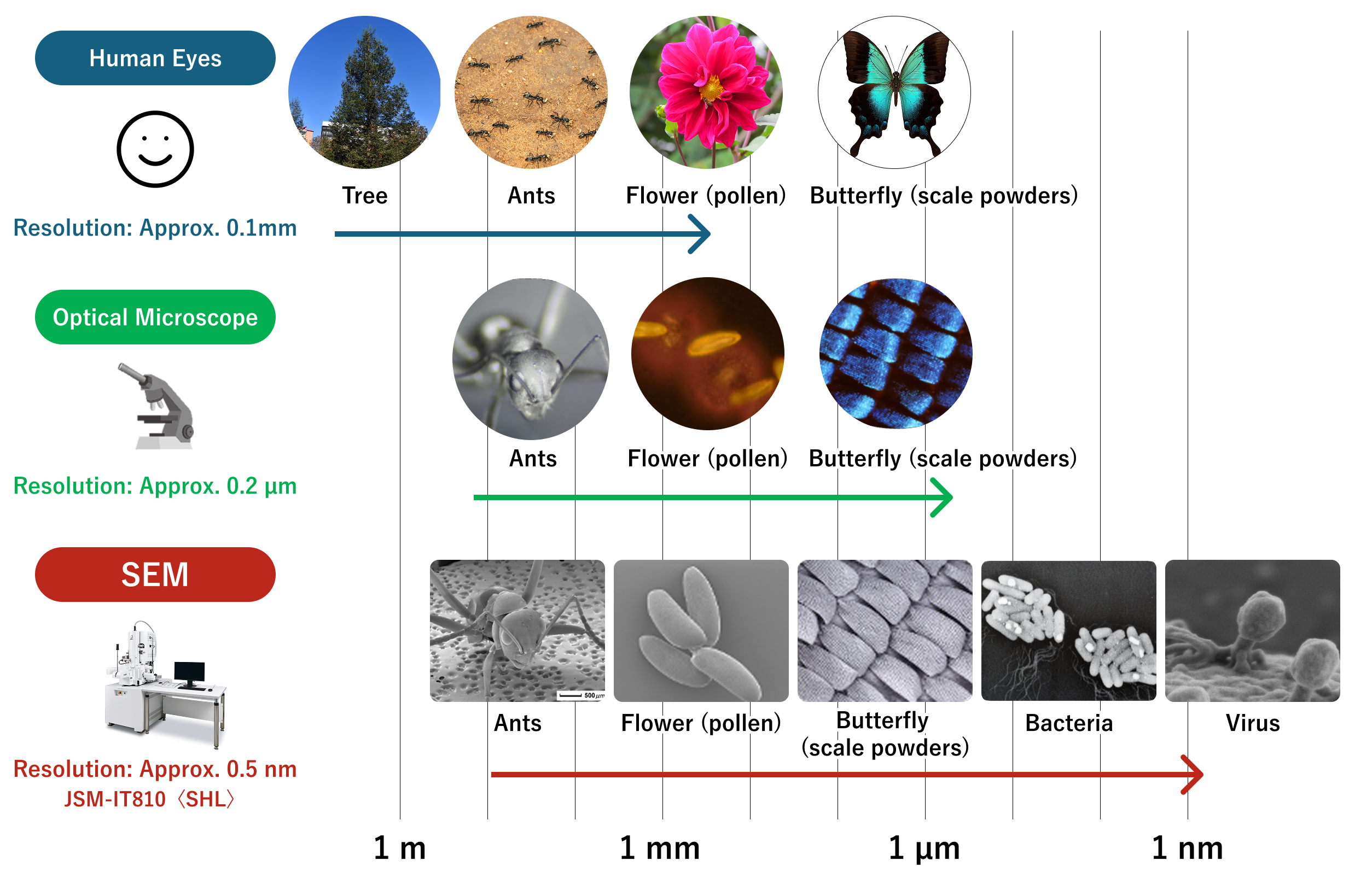
For example, while we can recognize the shapes of ants or flowers with the naked eye, we cannot see detailed
structures such as pollen or bacteria.
When an optical microscope is used, micron level structure of pollens, scale powders of insects can be
observed. Furthermore, when an electron microscope (SEM/TEM) is used, it is possible to capture nano-scale
structures such as bacteria and viruses with high precision.
Thus, depending on the type of microscopes to be used, the observable target and the depth of information
greatly differs.
In this article, we will explain the mechanisms and features of optical and electron microscopes, along with the key points for choosing the appropriate instrument depending on the purpose.
Differences between Optical Microscopes and Electron Microscopes
Comparison of mechanisms
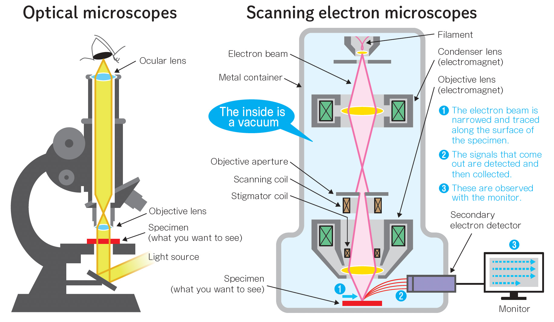
Mechanism of Optical Microscopes
Optical microscopes magnify the specimen with the objective lens and eyepieces made of glass by using visible light as a light source. Light either transmits or reflects the specimen, and is refracted by the lens on the way, to form an image. Users observe this image directly through the eyepiece. The magnification of an optical microscope is determined by multiplying the magnification of the objective lens by that of the eyepieces.
Mechanism of Electron Microscope
Electron microscopes are classified into Scanning Electron Microscopes (SEM) and Transmission Electron Microscopes (TEM). Here, we focus on Scanning Electron Microscopes (SEM).
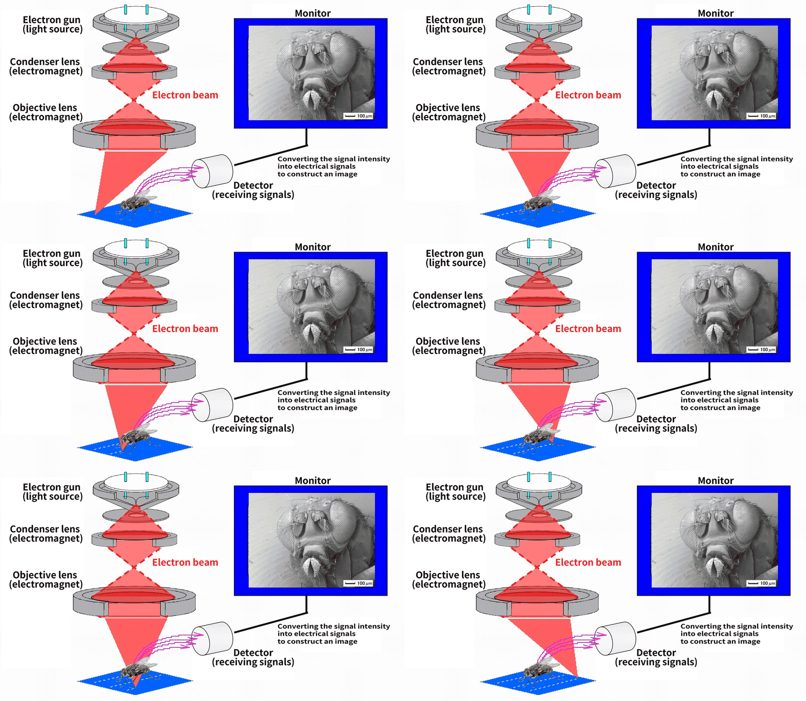
Scanning Electron Microscopes detect signals emitted from the surface such as secondary electrons and backscattered electrons, by scanning the specimen surface with finely focused electron beams, with electron beam as a light source, and display the enlarged image on the monitor. The path of the electron beam and specimen chamber are kept in a vacuum. Observation magnification is determined by the ratio between the scanning range (scan region) on the specimen and the image size displayed on the monitor. As magnification can be changed thorough scan control, continuous adjustment is possible from low to high magnifications.
Comparison of Features
| Optical microscope | Scanning electron microscope | |
|---|---|---|
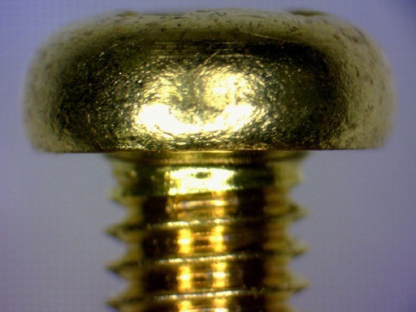
| Image specimen: screw Accelerating voltage:15 kV |
 |
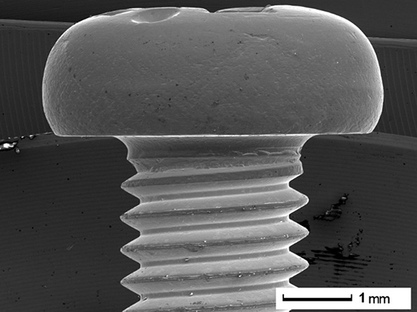 Accelerating voltage: 15 kV |
| Light source | Light | Electrons |
| Specimen chamber environment | Atmosphere | Vacuum |
| Color information | Color | None (monochrome) |
| Focal depth | Shallow | Deep |
| Observable size range | mm to µm | mm to nm |
| Elemental analysis | Not possible | Possible |
| Ease of operation | Relatively easy Widely used in education and general research |
Previously required expertise; now easier due to automation and improved UI |
Differences in Light Source and Observable Size
Electron microscopes use a short wavelength electron beam, while optical microscopes use long wavelength visible light to form the image. This 'difference in wavelength' results in a significant difference in resolution (i.e. how fine a detail can be distinguished). In general, the shorter the wavelength, the smaller the structure can be distinguished. Therefore, electron microscopes have far better resolution than optical microscopes.
Differences in Wavelength between Light and Electrons
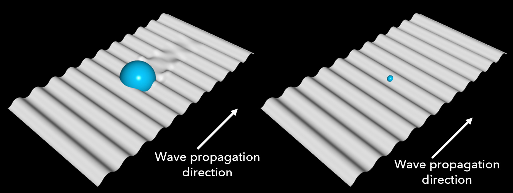
Left: Wavelength of Light (400 to 700 nm)
Right: Wavelength of Electron Beam (15 kV: 0.01 nm)
Shorter wavelengths allow observation of smaller structures. The resolution limit of a microscope is
roughly on the order of the wavelength used.
Differences in Specimen Chamber Environment
Optical microscopes enable observation in the natural environment in the atmosphere. Since they can capture the live cells and movement of microorganisms in real time, They are suitable for observing a wide range of specimens, including biological specimens, food, and oil.
On the other hand, electron microscopes are normally used in a vacuum, to avoid scattering of electron beam
in the air. Therefore, the specimen needs pretreatment such as drying, fixing, and addition of conductivity
(i.e. metal coating), etc.
However, recent SEMs are equipped with a low vacuum mode, and enable observation of non-conductive specimen,
moisture specimen, and plant without pretreatment.

SEM speedy observation and analysis without pretreatment!
- Application examples of
low-vacuum mode -
Would you like to try observing non-conductive (insulating) specimens in the SEM without any
pretreatment?
We introduce application examples of polymer materials, industrial materials, food, biological/plant
specimen using the JCM-7000 in low vacuum (LV) mode.
Differences in Color Information
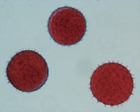
Optical Microscope Image (Approx. x 200)
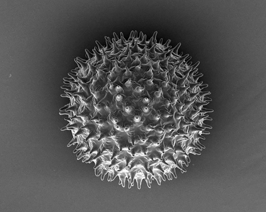
SEM Image (Approx. x 600)
Specimen: Pollen of Morning Glory
Optical microscopes can obtain an image with color, since they observe a specimen with visible light and glass lenses. In particular, for biological specimens, staining enhances differences in cells and tissues, helping to visually understand the specimen state.
On the other hand, Scanning Electron Microscopes (SEM) observe a specimen by using electron beams. The obtained image can be black and white. This is because electron beams have properties different from light, and are unable to capture information of color. Instead, electron microscopes can observe a microstructure that is difficult to capture with optical microscopes, at high resolution. For example, when observing pollen, an optical microscope is used to identify the differences in color and shape and determine the observation target and field of view. Then, an SEM is used to examine surface roughness and microstructure in detail, making the understanding more efficient and deeper.
Differences in Focal Depth
Focal depth means "the range that seems to be focused", which means, the width of depth of a clearly observable image.
In general, optical microscopes have less focal depth as the magnification increases. For a specimen with
roughness, only a part of the specimen comes into focus, and the entire image may seem blurred.
On the other hand, Scanning Electron Microscopes (SEM) have a very deep focal depth and even the image of a
specimen with a three-dimensional structure can come into focus in a wide range.
For example, this can be observed in the threads of the screw shown in the figure above.
The optical microscope image came into focus in a limited range only, and it is difficult to capture the
entire deep structure at the same time.
SEM image came into focus for the whole roughness and a clear three-dimensional image was obtained. When it
is required to capture the surface roughness and microscopic shape in detail, the excellent focal depth of
an SEM can serve as an advantage.
Differences in the Presence or Absence of an Elemental Analysis Capability
With the electron microscope, when an electron beam is irradiated to the specimen, the characteristic X-rays are emitted from the atoms near the surface of specimen.
By combining an Energy-Dispersive X-ray Spectrometer (EDS) or a Wavelength-Dispersive X-ray Spectrometer (WDS), it is possible to simultaneously observe the morphology of the specimen and identify the types of elements (qualitative analysis), measure their concentrations (quantitative analysis), and visualize their distribution (elemental mapping).
Differences in Operability
With optical microscopes, as an observation is possible simply by placing a specimen and adjusting focus, there is no need for special preparation or environmental adjustments. They are widely used in education and routine inspection.
On the other hand, conventional electron microscopes (SEMs) require management of the vacuum pump and Cooling water, and periodical maintenance. In addition, consideration was required for installation environments, such as vibration and electromagnetic wave interference. However, recently, compact general-purpose SEMs with excellent ease of operation and installation have become available. The hurdles for introduction and operation have been greatly lowered compared to the past. As a result, electron microscopes are now used not only in highly specialized R&D environments, but also in more accessible environments such as education and Quality Assurance.
Please check the installation case of table-top scanning electron microscope at a museum below:

A museum allowing visitors to experience electron microscopes, with smartphone-like operation
Ibaraki Nature Museum (Bando, Ibaraki prefecture) introduced a benchtop Scanning Electron Microscope (SEM) which can be operated by visitors. All operations necessary for observations are performed through a touch panel. It will provide an appealing new exhibition that will make children "want to go there again".
Benchtop Scanning Electron Microscope of JEOL【JCM-7000Plus NeoScope™】
As explained thus far, optical microscopes are easy to operate, and suitable for observation of biological specimens. On the other hand, SEMs can capture more microscopic structure at high resolution. Both have their own advantages. Needs such as "want to observe in more detail" and "operation must be simple" are addressed by JEOL's benchtop scanning electron microscope, the JCM-7000Plus NeoScope™
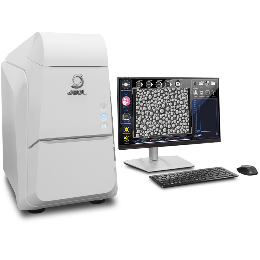
Benchtop Scanning Electron Microscope of JEOL【JCM-7000Plus NeoScope™】
"JCM-7000Plus NeoScope™" enables anyone to easily perform an observation of a microstructure and elemental difference that was not observable with optical microscopes. It is utilized in a wide range of fields, not only in research and development, but also Quality Assurance, and foreign substance analysis/material evaluation at fabrication sites.
Summary
Optical microscopes and electron microscopes each have their own principles and features. Using them separately based on the target and purpose enables a more effective analysis.
JEOL's "JCM-7000Plus NeoScope™" has been introduced in a variety of fields, as the tool enabling easy observation and analysis of microstructures and elemental information, without the need of special knowledge.
Please feel free to contact us for inquiries about installation and more detailed information.

JEOL Ltd.
Since its foundation in 1949, JEOL has been committed to the development
of cutting-edge scientific and metrology instruments, industrial and medical equipment.
Today,
many of our products are used throughout the world and we are highly regarded as a truly global
company.
Aiming to be a 'top niche company that supports science and technology around the
world', we will continue to respond precisely to the increasingly sophisticated and diverse needs
of our customers.