【DISCONTINUED】JXA-8530F Field Emission Electron Probe Microanalyzer
DISCONTINUED
This product is no longer available.
If you would like to know the latest information about your preferred product or to find out more about alternatives, please click on the link below. We hope you will continue to use our products.
JEOL revolutionized surface analysis with an EPMA featuring a field emission (FE) electron gun, and now is proud to present a new upgraded FE-EPMA. The JXA-8530F operates on PC Windows for data acquisition and analysis while maintaining the powerful hardware of the JXA-8500F including the FE electron gun, EOS, and vacuum system to achieve the ultra micro area analysis. User friendly, PC-based operation facilitate quick and easy analyses at the highest magnifications.
Features
A PC Controlled, WD/ED Combined System Opens Doors to New Ultra Micro Analysis
PC Control
EPMA Quick Start
User's Recipes
'Click Point Analysis'
Real time display of mixed X-ray images (WDS)
EDS spectral imaging
New analyzing crystal for ultra light elements
Notices:Windows is a registered trademark of Microsoft Corporation in the United States and other countries.
High spatial resolution in X-ray mapping with the FE electron gun
The FE electron gun produces a probe that is only1/2 to 1/10 the size of that produced in a thermionic-emission electron gun in a conventional EPMA, usinga W filament or a LaB6tip.
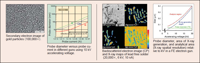
The FE electron gun is capable of producing a micro probe at low accelerating voltage even with high probe curren-ts(10 to 100 nA), allowing for WDS analyses with high X-rayspatial resolution.
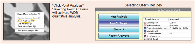
"Click Point Analysis", User's Recipes
"Click Point Analysis" allows the user to acquire qualitative WDS spectra and semi-quantitative analyses simply by clicking a point on a secondary electron or backscattered electron image. User's Recipes provides for easy access to preset analytical conditions. These features are designed to maximize the efficiency of the FE-EPMA with the simplest of operations.
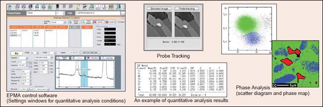
Advanced Operation
A user can design detailed analytical procedures tailored to their research objective, such as complex quantitativeelemental analysis of nano-size areas. Also integrated into the system are a complete line of applications and easy-to-use software packages that provide for extensive data analysis methods and tools. For example, Probe Tracking isprovided making it easier to perform long duration area and spot analyses on extremely small features without concernfor beam drift.
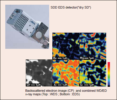
Combined WD/ED System
The JXA-8530F has a user friendly combined WD/ED system incorporating JEOL's advanced WDS and EDSdetectors. Combining the WDS for trace element ana-lysis and JEOL's proven EDS, the JXA-8530F is a po-werful tool for efficient data acquisition of quantitative analyses, high magnification beam scan mapping, andlarge area stage scan mapping.
Specifications
| Detectable element range | WDS: (Be※) / B~U,EDS: B~U |
|---|---|
| Detectable X-ray range | Detectable wavelength range with WDS : 0.087 to 9.3nm Detectable energy range with EDS : 20keV |
| Number of spectrometers | WDS: Up to 5 selectable, EDS: 1 |
| Maximum specimen size | 100 mm × 100 mm × 50 mm (H) |
| Accelerating voltage | 1 to 30 kV (0.1 kV steps) |
| Probe current range | 10-12 to 5×10⁻⁷ A |
| Probe current stability | ± 0.3 % /h |
| Secondary electron image resolution | 3 nm (W.D. 11 mm, 30 kV) |
| Minimum probe size | 40 nm (10 kV, 1×10⁻⁸ A) 100 nm (10 kV, 1×10⁻⁷ A) |
| Scanning magnification | × 40 to × 300,000 (W. D. 11 mm) |
| Scanning image resolution | Maximum 5,120 × 3,840 |
| Color display | For EPMA analysis : LCD 1,280×1,024 For SEM operation and EDS analysis : LCD 1,280×1,024 |
With optional analyzing crystal for Be analysis
Application
Application JXA-8530F
Analysis of Cracks in Brass Piping Parts
Micro Area Analysis with JXA-8530F (FE-EPMA)
More Info
Are you a medical professional or personnel engaged in medical care?
No
Please be reminded that these pages are not intended to provide the general public with information about the products.