Review SEM
Review SEM
Review SEM is an inspection system to detect, classify and map foreign materials and defects (scratches, pattern failures, etc.) on a semiconductor wafer surface, which occur in semiconductor manufacturing processes consisting of several thousands of steps (step means a smallest unit of process). The Review SEM serves to improve the yield of fabrication of chips (finely divided area on the wafer) and reliability of the fabricated chips. The size of the foreign materials and defects to be detected by the Review SEM, is approximately half the minimum line width of the chip manufacturing process.
In the early stages, the foreign materials and defects were identified by detecting differences in light scattering on the wafer surface. However, from around 1990 the minimum processing dimension reached down to 500 nm due to device miniaturization, and the foreign materials and defects to be inspected became smaller than 200 nm. Since then, the inspection system was replaced from the optical to SEM system. Furthermore, entering into 2020s, the minimum processing dimension became 5 to 10 nm, and a high image resolution of 2 nm or better was required for detecting very-small foreign materials and defects of interest. For this reason, SEMs equipped with a semi-in-lens objective lens and a retarding function (a type of deceleration methods), which are suited to high-resolution observation, are currently used.
In order to shorten the throughput of the inspections, the Review SEM can be used for (1) inspections specifying five to several tens of areas on the wafer instead of inspecting the entire surface of a 300 mm diameter wafer, and (2) inspections of the limited processes, where the foreign materials and defects give significant effects on the yield of the chips, such as transistor gate processing, contact hole etching and fine-pitch wiring layer patterning.
In many cases, transistors and capacitors are already fabricated on the wafer at the time of inspection by the Review SEM. Thus, the acceleration voltage is kept at around 0.5-0.7 kV to prevent incident electrons from affecting the device characteristics of the transistor. In order to collect information on shape and composition, an in-column detector is used, which can efficiently collect secondary and backscattered electrons.
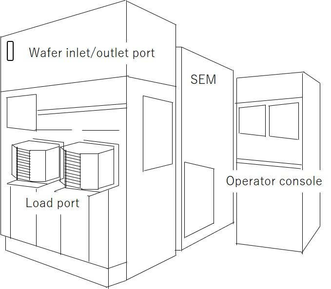
Fig. 1 illustrates a schematic of a typical Review SEM instrument. The load port is placed at the front of the instrument to insert wafers automatically transported from the manufacturing equipment for deposition and etching into the Review SEM (input), and to remove wafers from the instrument after finishing the measurement (output). Wafer inspection is carried out automatically according to the recipe (specific procedure defined by the industry standard), thus, usually there is no operators but an operator console is provided for maintenance of the instrument. The SEM column is covered by an enclosure to protect the column from vibrations due to air flow and noise.
Fig. 1. Schematic of the external view of a Review SEM system.
The Review SEM system has following features.
The system is equipped with a specimen stage enabling observation of the entire surface of a 300 mm diameter wafer.
The system is connected to a wafer transfer system placed in the front-end process unit. The introduction of the inspected wafer, inspection, output of inspection results and transfer (output) of the wafers to the next process are fully automated.
Inspection results are transferred to a server which manages the data of manufacturing processes, using the format and communication system specified by “SEMI Standards”, the industry standard.
Wafers having a higher number of defects than the user’s pre-defined criteria are not transferred to the next process, but are subjected to standby.
The system can record and map the positional coordinates of defects, classify the defects by shape and composition, and compare the distribution of foreign materials between the other wafers by mapping.
When inspecting the wafer chip surfaces on which circuit patterns are formed, defects are displayed by detecting the difference between the results of observation of the same area of the adjacent chip.
The system is equipped with an inspection function that detects high resistance areas in contact holes (vertical holes filled with a metallic material that connect the upper and lower wiring layers and transistors) using changes in image quality due to charging (voltage contrast).
The Review SEM is made so that yield and reliability are not affected by foreign materials and defects generated during inspection, as with the other inspection systems.
Fig. 2 shows an example of detection of foreign materials using a Review SEM. There are two types of foreign materials in this example. Foreign materials containing many heavy elements (e.g. metals) are displayed by blue dots, and foreign materials consisting of relatively light elements (mainly Si) are displayed by red dots. Heavy elements often originate from a semiconductor manufacturing equipment and light elements from the manufacturing processes (process reactions).
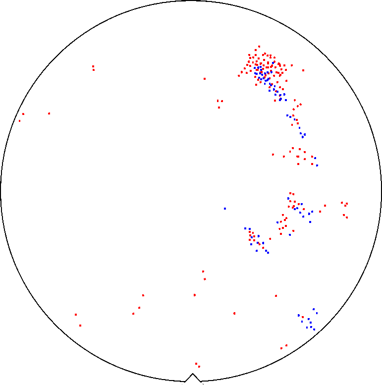
Fig. 2. Example of mapping foreign materials detected using a Review SEM.
Positional information of the detected foreign materials, classified by shape, and composition, is displayed as a map.
Related Term(s)
Term(s) with "Review SEM" in the description

Are you a medical professional or personnel engaged in medical care?
No
Please be reminded that these pages are not intended to provide the general public with information about the products.