coating, metal coating
coating, metal coating
Coating is to cover the surface of a nonconductive specimen with a conductive thin-film (carbon or metal) of a few nm to 10 nm thick. If the incident electrons that enter a specimen are accumulated in a specimen, the specimen surface is negatively charged. If more secondary electrons are emitted from the specimen than the entering electrons, the specimen surface is positively charged.
When a conductive thin-film is coated, the extra electric charges escape to ground, and then distortion of the secondary electron image due to charging and image anomalies such as extremely light (or dark) images of local areas disappear. If the specimen is conductive, the coating is not needed.
Fig. 1 shows an example of SEM images taken from a human hair with gold (Au) coating and without coating. The Au-coated hair obtains conductivity and the scale patterns of the surface can be observed without image distortion (Fig. 1 (a)). On the other hand for the case of no coating, the hair is seen to be thinner than its actual thickness due to the deflection of the incident electron beam caused by charging. In addition, the charging causes the center region of the hair abnormally dark and the scale patterns of the hair surface cannot be seen clearly (Fig. 1 (b)).
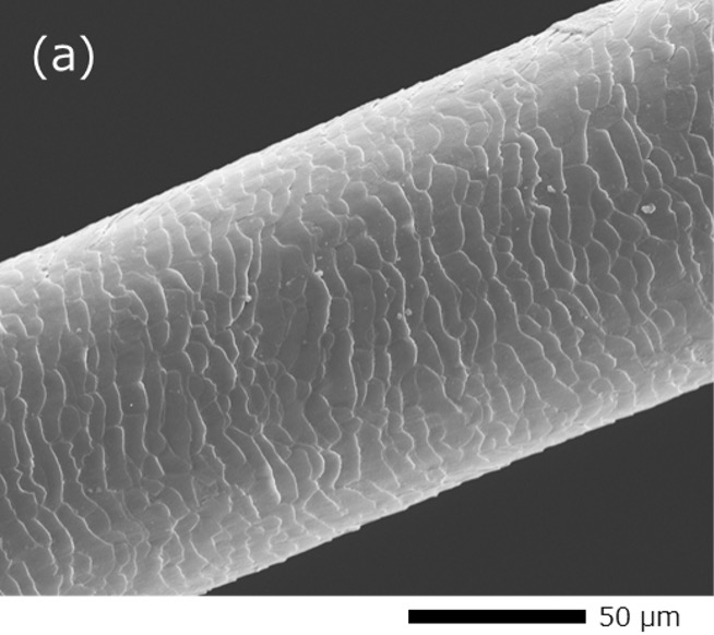
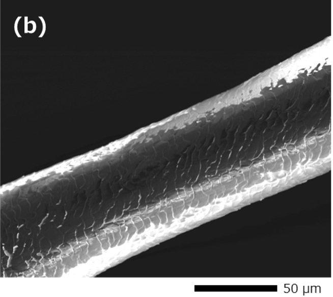
Fig. 1 Comparison of SEM images with and without coating.
(Instrument: JCM-7000, Accelerating voltage: 15 kV)
(a) Secondary electron image of a human hair with gold (Au) coating. The scale patterns of the surface are clearly seen without image distortion. It is noted that the Au film causes no effect on the observation of the morphology of the hair because of its thin thickness of only a few nm.
(b) Secondary electron image of a human hair without coating. The hair is seen to be thinner than its actual thickness due to the deflection of the incident electron beam caused by charging. The center region of the hair appears abnormally dark due to charging and the scale patterns of the hair become unclear.
Table 1 Coating methods and materials
| Coating method | Vacuum evaporation | Sputtering | Plasma CVD | |
|---|---|---|---|---|
| Material | Carbon (C) | Gold (Au) | Platinum (Pt) | Osmium (Os) |
| Particle | No particle is seen in a SEM image. | Particles (a few 10 nm size for a particle) are seen. | Particles (a few nm size for a particle) are seen. | No particle is seen in a SEM image. |
| Uniformity of coating | Vacuum evaporation (C) < Sputtering (Au, Pt) < Plasma CVD (Os) | |||
| Suitable specimen | All specimens for elemental analysis | All specimens for SEM observation | Complex-structure specimens (e.g. porous materials, biological specimens, fibers) | |
| Magnification range used for observation & analysis | 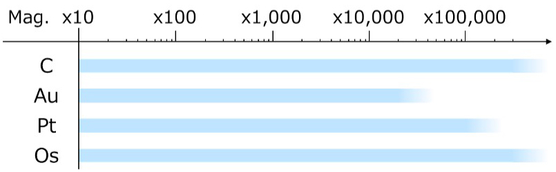 |
|||
Table 1 lists the coating methods and the characteristics of materials used for each coating. The coating methods used are vacuum evaporation, sputtering and plasma CVD (chemical vapor deposition). The coating materials available for each coating method are different; carbon (C) is used for vacuum evaporation, gold (Au) and platinum (Pt) for sputtering, and osmium (Os) for plasma CVD. The coating material is likely to reach and cover the backside surface of the specimen in the order of vacuum evaporation < sputtering < plasma CVD.
Carbon is suitable for elemental analysis. This is because the Kα line (0.27 keV) of the EDS spectrum of carbon hardly overlaps with the peaks originating from the other constituent elements of a specimen and carbon hardly absorbs characteristic X-rays generated from the specimen.
Au, Pt and Os, whose atomic numbers are respectively 79, 78 and 76, produce their EDS spectral peaks close to each other. It should be noted that the Mα lines (1.9 to 2.4 keV) of Au, Pt and Os overlap with the Kα line (2.0 keV) of phosphor (P), the Kα line (2.3 keV) of sulfur (S) and the Lα line (2.0 keV) of zirconium (Zr).
Thus, those coating materials are better not be used in the analysis of specimens that may contain P, S, and Zr.
Comparing Au and Pt, it is better to use Pt because Pt particles are smaller than Au particles. Fig. 2 shows a comparison example of SEM images of carbon black (soot particles) in three cases; without coating, with Au-coated and with Pt-coated. In Fig. 2(a), no metal particle is seen on carbon black. In Fig. 2(b), Au particles with a size of a few 10 nm are seen. In Fig. 2(c), Pt particles are hardly visible at this magnification and are only a few nm in size.
As seen in Fig. 2(c), since Pt particles are hard to be seen even at high magnifications, Pt coating can be used for specimens with a size of a few μm or less (e.g. nano-particles, resist patterns and insulating films of semiconductors). For even higher-magnification SEM observation, chromium (Cr) or iridium (Ir), which has a smaller particle size than Pt, can be coated by sputtering.
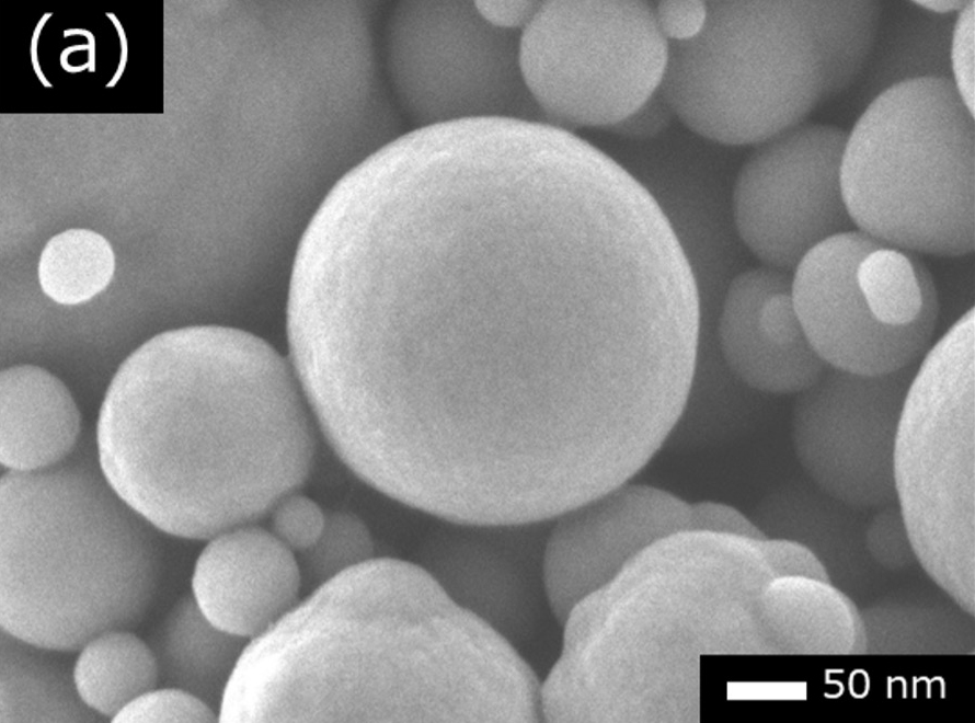
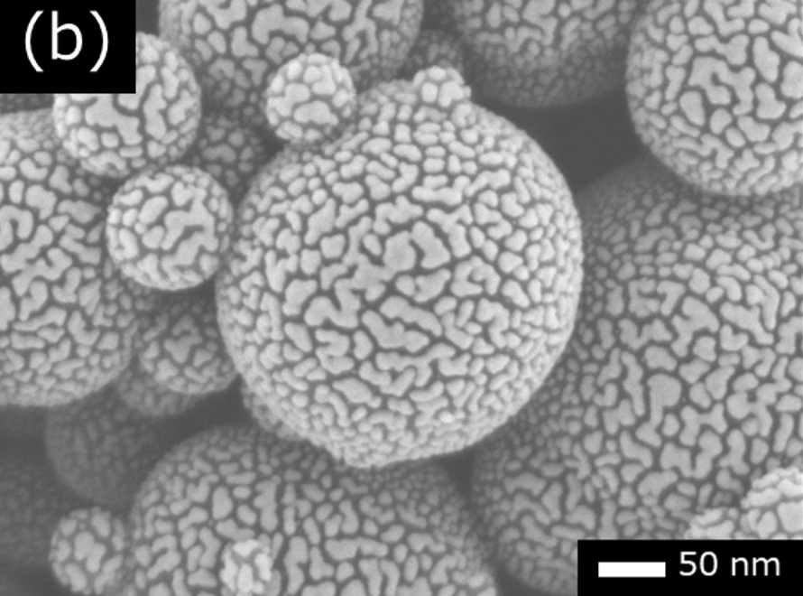
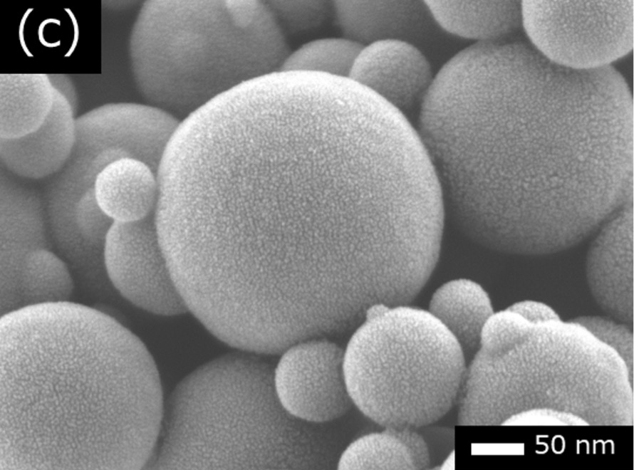
Fig. 2 Comparison of granularity with gold (Au) and platinum (Pt) coatings.
(Instrument: JSM-IT800SHL, Accelerating voltage: 1.5 kV)
(a) Secondary electron image of carbon black without coating. No particle is seen on the surface of carbon black.
(b) Secondary electron image of carbon black with Au-coated. The particle size of Au is a few 10 nm.
(c) Secondary electron image of carbon black with Pt-coated. The particle size of Pt is a few nm.
Plasma CVD using osmium tetroxide (OsO4) is suitable for complex-structure specimens such as porous materials, biological specimens and fibers, as it enables uniform coating for not only the top surface of a specimen but also the side and bottom surfaces. However, it should be noted that OsO4 is toxic and must be handled with special care. A filter must be set in the coating system to absorb and remove OsO4 gas to prevent the leakage of the gas to outside.
Related Term(s)
Term(s) with "coating, metal coating" in the description
Are you a medical professional or personnel engaged in medical care?
No
Please be reminded that these pages are not intended to provide the general public with information about the products.