backscattered electron image, BSE image
backscattered electron image, BSE image
"Backscattered electron image" means an image formed by backscattered (reflected) electrons which are emitted by elastic scattering of the incident (primary) electrons. A backscattered electron image reveals the compositional difference in a specimen (difference in the average atomic number). Its spatial resolution is low in comparison with that of the secondary electron image. The edge contrast does not occur, which appears in the secondary electron image. The backscattered electron image is less affected by electric charging on the specimen surface than the secondary electron image because the backscattered electrons have a high energy.
The backscattered electron emission rate (coefficient) greatly changes for the atoms with an atomic number up to 40. Thus, the backscattered electron image is sensitive to a small difference of atomic number for a specimen with such atomic numbers. For example, for a specimen with an atomic number near 30, if the difference in average atomic number is more than 0.2 to 0.3, a sufficient difference in the image contrast can be recognized. Specifically, each atom can be identified for brass composed of Cu (29) and Zn (30), and for a compound semiconductor of Ga (31) and As (33).
In general, the spatial resolution of the backscattered electron image is worse than that of the secondary electron image, namely several times to one order of magnitude lower. The reason for this is as follows. Although secondary electrons are emitted from a small depth of only 10 nm from the surface, the backscattered electrons are emitted from a large depth of a few micrometers from the surface (depending on the accelerating voltage of the incident beam). This gives rise to a large diffusion for the backscattered electrons until to reach the specimen surface, resulting in a low resolution. However, the recent high-resolution SEM enables the detection of backscattered electrons even for the incident electron energy as low as 1keV or less. Thus, the diffusion region of the backscattered electrons is suppressed extremely small, and then, the backscattered electron image produces a high resolution comparable to that of the secondary electron image taken by the same incident electron energy.
The backscattered electron image also shows the topography of the specimen surface. When an uneven specimen is observed, a shadow is produced on one side of a tilted face, enabling acquisition of a stereoscopic (shadow) image.
However, an edge-emphasized image formed by secondary electrons cannot be obtained due to the diffusion effect of the backscattered electrons.
Fig. (a) shows a set of a secondary electron image and a backscattered electron image of the letter-printed part on a name card. Since the ink of letters contains heavy metals, the backscattered electron image shows a brighter contrast than that of the fiber part of the name card (compositional contrast). The compositional contrast is not seen in the secondary electron image. It is noted that, the surface of this specimen is carbon-coated to avoid electric charging.
Fig. (b) shows a set of a secondary electron image and a backscattered electron image of the surface of an electrode of a card-edge connector. The backscattered electron image reveals the specimen topography stereoscopically owing to a strong oblique illumination effect. It should be noted that the secondary electron image does not show the stereoscopic contrast.
It is noted in addition, for a crystalline specimen with a uniform composition, the backscattered electron image shows so-called the electron channeling contrast due to a difference in crystal orientation.
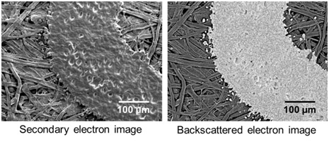
Fig. (a) Comparison of a secondary electron image (left) and a backscattered electron image (right) of the letter part of a carbon-coated name card (seen at the center of both images), taken at an accelerating voltage of 15 kV.
In the backscattered electron image, the letter part appears very bright (compositional contrast).
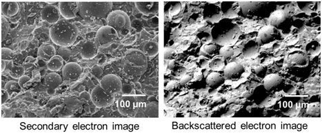
Fig. (b) Comparison of a secondary electron image (left) and a backscattered electron image (right) of the surface of an electrode of a card-edge connector, taken at an accelerating voltage of 10 kV.
In the backscattered electron image, topographic details of the specimen are stereographically observed owing to a strong oblique illumination effect (topographic contrast).
Related Term(s)
Term(s) with "backscattered electron image, BSE image" in the description
Are you a medical professional or personnel engaged in medical care?
No
Please be reminded that these pages are not intended to provide the general public with information about the products.