secondary electron image, SE image
secondary electron image, SE image
“Secondary electron image” means an image formed by detecting secondary electrons which are generated from the constituent atoms excited by inelastic scattering of the incident (primary) electrons in a specimen. An SEM image generally indicates a secondary electron image, and the image reveals fine surface structures (topographic details) of the specimen. Since the energy of the secondary electron is several 10 eV or less, only the electrons generated within 5 to 10 nm from the surface are emitted in vacuum, beyond the specimen. Thus, the secondary electron image provides high spatial-resolution and is very sensitive to the top-surface structure of the specimen. However, since the energy of the secondary electron is low, image blur is likely to arise, caused by a charging on the specimen surface.
Increasing the specimen tilt angle increases the emission amount of secondary electrons beyond the specimen surface, thus producing contrast depending on the specimen shape. Furthermore, from small protrusions or sharp topographic regions on the specimen, the emission amount of the secondary electrons increases remarkably, leading to further brighter contrast of the image. This contrast is called the edge effect characteristic of the secondary electron image and enables clear observation of the fine surface structure.
Fig. (a) shows a secondary electron image of crystalline particles of trioxide tungsten. The image reveals the shape of the crystalline particles due to the different emission amount of secondary electrons caused by different inclination of the surfaces of crystalline particles. The edge regions are seen to be particularly bright (edge effect) while the edge effect is confirmed.
The image resolution is 0.6 nm to 3 nm for an accelerating voltage of an incident electron probe of 15 kV. The main factor that determines the resolution is the diameter of the incident electron probe. W (tungsten) or LaB6 is normally used for the electron source (gun). To obtain a smaller electron-probe diameter, a field emission gun (FEG) that has a smaller electron source is used.
For observing a clear image, it is effective to decrease the accelerating voltage. At low accelerating voltages, the diffusion region of the incident electrons into the specimen is small. Thus, the image is formed by secondary electrons excited near the surface, resulting in clear imaging of the fine surface structure of the specimen. However, when the accelerating voltage is lowered, the chromatic aberration of the electron lens increases, leading to the degradation of the resolution. Thus, to use a lens with a small aberration is desirable. To the contrary at high accelerating voltages, the diffusion region of the incident electrons becomes large, and thus, the contribution of the secondary electrons generated in a region distant from the incident electron path becomes large. As a result, the obtained image becomes unclear and the fine surface structure of the specimen is difficult to view. Decreasing the accelerating voltage increases the aberration of the objective lens and the probe diameter becomes large. But in the present SEM, the improvement of the objective lens enables a sufficiently small probe diameter to be obtained even at an accelerating voltage of as low as 5 kV.
In Fig. (b), two secondary electron images are compared, where a gold-coated filter paper is observed at accelerating voltages of 5 kV and 30 kV, respectively. At a voltage of 5 kV, the image shows high contrast and the surface structure is clearly observed. At a voltage of 30 kV, the image is degraded and the details of the surface structure are unclear.
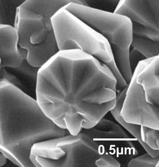
Fig. (a) Secondary electron image of crystalline particles of trioxide tungsten, taken at an accelerating voltage of 10 kV.
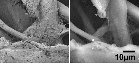
Fig. (b) Comparison of secondary electron images (same field of view) of a gold-coated filter paper taken at accelerating voltages of 5 kV (left) and 30 kV (right).
Low accelerating-voltage is suitable for observation of fine surface structure (topographic details).
Term(s) with "secondary electron image, SE image" in the description
Are you a medical professional or personnel engaged in medical care?
No
Please be reminded that these pages are not intended to provide the general public with information about the products.