deceleration method
deceleration method
A method of decelerating the incident electron beam just before a specimen using an electric field, so as to maintain a high spatial resolution of the SEM image at a low accelerating voltage. The method is particularly effective in maintaining high spatial resolution for the low-accelerated electron beam of ~1 keV or less. The low-accelerated electron beam is used to observe the top surface of a specimen, and to observe specimens which are easily damaged by a high-accelerated electron beam, such as polymer materials, and specimens which are easily electrically charged.
There are two methods of generating an electrostatic field to decelerate the incident electron beam (hereinafter, called "deceleration field"): the retarding method and boosting method (Fig. 1). In the boosting method, the accelerating tube has to be placed in the microscope column. In the retarding method, the incident beam can be decelerated by applying a potential directly to the specimen without installing the accelerating tube. For a high spatial-resolution SEM observation at an extremely low accelerating voltage of a few 100 V, the retarding method is used in addition to the boosting method. The two methods are explained for the examples shown in Fig. 1, where the electron beam is decelerated from 3 keV down to 1 keV.
In the retarding method (Fig. 1 (a)), a negative voltage of -2 kV is applied to the specimen. An electron beam emitted at 3 keV passes through the objective lens at 3 keV, and then the electron beam is decelerated down to 1 keV between the objective lens and specimen.
In the boosting method (Fig. 1 (b)), a positive voltage of +2 kV is applied to the accelerating tube placed in the microscope column. An electron beam emitted at 1 keV is accelerated up to 3 keV in the accelerating tube and passes through the objective lens at 3 keV. Then, the electron beam is decelerated down to 1 keV between the exit of the accelerating tube and the lower pole of the objective lens, and then reaches the specimen.
When using the deceleration method, 1) The incident electron beam passes though the magnetic field of the objective lens at a high voltage and thus, the chromatic aberration of the objective lens is reduced, leading to a decrease of the electron-probe diameter. 2) The deceleration field acts as an additional convex lens and thus, the center (principal plane) of the entire lens comes closer to the specimen, leading the probe diameter even smaller. 3) The chromatic aberration of the electrostatic lens increases the probe diameter.
The effects of 1) and 2) contribute to improve the spatial resolution of the SEM image. In particular, the effect of 1) contributes significantly to the improvement of the spatial resolution.
Fig. 2 schematically shows the trajectories of the electron beam for (a) no deceleration filed, (b) the retarding method, and (c) the boosting method. When the deceleration method is used, the electron beam passes through the magnetic objective lens at 3 keV (not 1 keV) and is then decelerated to 1 keV by the electrostatic field, and converges onto the specimen. To maintain the energy of the electron beam high in the magnetic lens allows the chromatic aberration of the magnetic lens to be small. Furthermore, as the electron beam travels through the deceleration field, the beam is decelerated and converges onto the specimen plane with increasing the inclination of the electron trajectory. In each figure (a and b), the intersection point of the dashed line A extending the incident beam with the tangential line (dashed line B) of the trajectory on the specimen plane, gives the position of the principal plane. The deceleration field lowers the principal-plane of the lens and shorten the focal length, increasing the demagnification ratio of the lens.
Table 1 lists the calculated electron-probe diameters d and the magnitudes of their components do,, dc,, dd, ds achieved for the three models shown in Fig. 1 and Fig. 2. In the case of imaging with a low acceleration energy of 1 keV with no deceleration field, the probe diameter is almost determined by the diameter components of chromatic aberration dc and diffraction aberration dd [1]. When the deceleration method is used, dc decreases owing to the decrease of chromatic aberration of the objective lens. Furthermore, since the demagnification ratio (convergence angle) is increased, the electron source component d0 and diffraction aberration component of dd. decrease.
In the retarding method, if the specimen is uneven or tilted, the electric field in front of the specimen can be disturbed and then, a degradation of resolution may occur and anomalous contrast may arise.
Combining the bosting method and the retarding method, the highest spatial-resolution SEM image (the smallest probe diameter) can be obtained at extremely low accelerating voltages of a few 100 V.
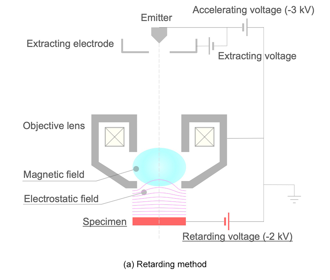
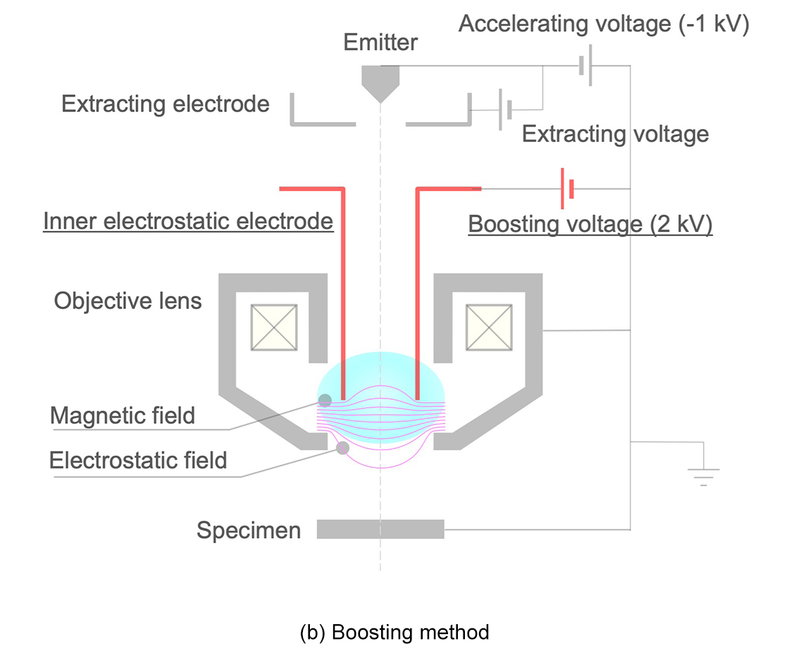
Fig. 1 Two deceleration methods (schematics)
The case of an electron beam being decelerated from 3 keV down to 1 keV is shown.
(a) Retarding method. A negative voltage (-2 kV) is applied to the specimen with respect to the objective lens, and a deceleration field is generated between the lower pole of the objective lens and the specimen.
(b) Boosting method. A positive voltage (2 kV) is applied to the accelerating tube in the electron-beam path, and a deceleration field is generated between the lower end of the tube and the lower pole of the objective lens. The boosting method requires a dedicated instrument with an accelerating tube.
A combined use of the boosting and retarding methods is possible if the instrument with the accelerating tube is designed to make it possible to apply a potential to the specimen.
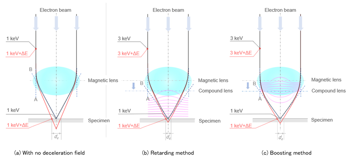
Fig. 2 Electron-beam trajectories in the deceleration methods (landing electron-beam energy: 1 keV)
The electron-beam trajectories for the landing electron-beam energy of 1 keV and of 1 + ΔE keV are respectively shown by black lines and red lines. (a) Without the deceleration method. (b) With the retarding method and (c) with the boosting method. (a) When the deceleration method is not used, the principal plane of the lens is located on the dashed line labelled as "Magnetic lens" in the figure. The shift between the black line and red line is due to the shift of the focal point caused by the chromatic aberration of the lens. The size (width) of the red line on the specimen corresponds to the probe-diameter component due to the chromatic aberration. The position of the principal plane of the compound lens composed of the magnetic field and the electrostatic field, each shown in (b) and (c), is on the dashed line labelled as "Compound lens" in each figure. The position of the principal plane using the deceleration method, is shifted downward from the position without the deceleration method (a). The deviation between the black line and red line shown in (b) and (c) is smaller than that from (a). This indicates that the chromatic aberration is reduced when the deceleration method is used. The convergence angle of the electron beam onto the specimen is determined by the tangential line of the electron trajectory (black line) at 1 keV on the specimen plane. When the deceleration method is used, the convergence angle increases owing to the lens action by the deceleration field.
Table 1 Calculations of the electron-probe diameters without the deceleration method and with two deceleration methods †
| Probe diameter component [nm] | Without deceleration field | Retarding method | Boosting method |
|---|---|---|---|
Electron source component ![do = Mdss [nm]](./glossary_file/file/deceleration-optics_4.png) |
8.3 | 6.0 | 5.9 |
Diffraction aberration component ![dd = 0.61λ⁄sinα [nm]](./glossary_file/file/deceleration-optics_5.png) |
6.9 | 5.0 | 4.9 |
Spherical aberration component ![ds = 0.5Csα3 [nm]](./glossary_file/file/deceleration-optics_6.png) |
0.68 | 0.79 | 0.76 |
Chromatic aberration component ![dc =Cc ∆E⁄Eα [nm]](./glossary_file/file/deceleration-optics_7.png) |
11 | 4.8 | 6.9 |
Electron-probe diameter ![d = √(d02+dd2+ds2+dc2) [nm]](./glossary_file/file/deceleration-optics_8.png) |
15 | 9.3 | 10 |
† Here, M is the demagnification ratio, dss is the electron source size, λ is the wavelength of the electron, α is the convergence angle, ΔE is the energy spread of the electron, and E is the energy of the electron.
[1] It is noted that the chromatic aberration and diffraction aberration are dominant at a low accelerating voltage condition (see Fig. 2 of "electron-probe diameter" in "Glossary of SEM Terms." of JEOL Web site).
Related Term(s)
Term(s) with "deceleration method" in the description
Are you a medical professional or personnel engaged in medical care?
No
Please be reminded that these pages are not intended to provide the general public with information about the products.