chromatic aberration
chromatic aberration
The chromatic aberration causes a spread of electron beams on the focal plane of the objective lens due to the difference in the focal positions for the electron beams with different energies.
The monochromatic electron beams having the same energy E converge onto a point of the focal plane of the objective lens. However, if the electron beams have an energy spread, the beams do not converge on one point but converge on front or rear the focal plane depending on the energy difference ±ΔE, as is shown schematically in Fig. 1. The tracks of the electron beams with energy E, with energy E+ΔE/2, and with energy E–ΔE/2, are respectively drawn by black, blue and red lines. When the energy spread is ±ΔE/2 with respect to E, the smallest diameter dc (minimum confusion circle) of the electron probe on the focal plane is given by dc = CcαΔE/E.
Here, α is the convergence semi-angle of the electron beam with energy E, and Cc is the proportional factor of ΔE/E, called "chromatic aberration coefficient" of the objective lens. Cc is a function of the distance between the objective lens and specimen (working distance, WD). As shown in Fig. 2, Cc monotonically increases with increasing WD.
The energy spread ΔE is different for the types of the electron gun of the SEM instrument. For a thermionic-emission electron gun with a tungsten filament, ΔE is 1 to 3 eV. For a Schottky emission electron gun, ΔE is 0.5 eV. For a cold field-emission electron gun (CFEG), ΔE is 0.3 to 0.4 eV. The accelerating voltage of an ordinary SEM ranges between 0.5 kV and 30 kV. As the accelerating voltage is lower, the chromatic aberration becomes larger, giving to a larger electron probe diameter dc.
In the out-lens type objective lens, WD is usually set at about 10 mm. When Cc and α are assumed respectively as 20 mm and 5 mrad, dc is calculated to be 5.0 nm at an energy spread ΔE = 1 eV for the tungsten filament of the thermionic-emission electron gun.
※1 L. Reimer, Scanning Electron Microscopy, Springer, Berlin, Germany, p. 24 (1998).
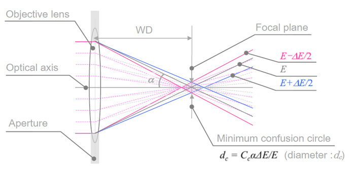
Fig. 1 Schematic diagram of the spread of electron beams due to chromatic aberration of the objective lens
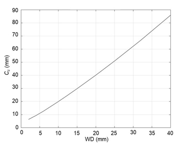
Fig. 2 Relationship between the working distance WD and chromatic aberration coefficient Cc
Related Term(s)
Term(s) with "chromatic aberration" in the description
Are you a medical professional or personnel engaged in medical care?
No
Please be reminded that these pages are not intended to provide the general public with information about the products.