4 dimensional-scanning transmission electron microscopy, 4D-STEM
4 dimensional-scanning transmission electron microscopy, 4D-STEM
Four dimensional-scanning transmission electron microscopy (4D-STEM) is a method in scanning transmission electron microscopy (STEM) that acquires the diffraction patterns for many probe points using a two-dimensional (2D) detector (pixel array STEM detector), creates four-dimensional (4D) data and obtains electron microscope images reflecting information from the diffraction patterns.
That is, an electron probe is scanned two-dimensionally on a specimen, and electron diffraction patterns are simultaneously recorded at each specimen position using a two-dimensional (2D) detector (Fig. 1(a)). The acquired data forms a four-dimensional (4D) data consisting of the 2D spatial position data of the specimen (x, y) and the 2D diffraction data (u, v) corresponding to each spatial position formed on the camera screen (Fig. 1(b)). From this 4D data, it is possible to visualize the distribution of crystalline phases, crystal orientations, and the directions of magnetic- and electric-fields by using the differences in the diffraction data (u, v) at specific 2D positions (x, y). It is also possible to visualize positional changes in the crystal structure by using the angle-dependent intensities of the diffraction patterns, which have not been fully used in the conventional STEM method. Fig. 2 illustrates the difference of the convergence angle of the electron probe when taking diffraction patterns. In Fig. 2(b), the adjacent diffraction disks are partially overlapped with each other. From the overlapping areas, the phase of the corresponding diffracted wave is obtained. This phase is then used to refine the structure of the specimen, which is known as ptychography. Collectively, these techniques are referred to as the 4D-STEM method.
Three analysis examples using 4D-STEM are presented below. In each case, the convergence angle of the electron beam (probe) and the magnification by the image-forming system (camera length) are different (Fig. 2). These conditions are determined according to the purpose of analysis
Example of orientation analysis of a crystalline specimen (Fig. 3).
Example of reconstruction (phase reconstruction) of a crystal structure using ptychography (Fig. 4).
Example of visualizing the magnetic field distribution in a specimen (Fig. 5).
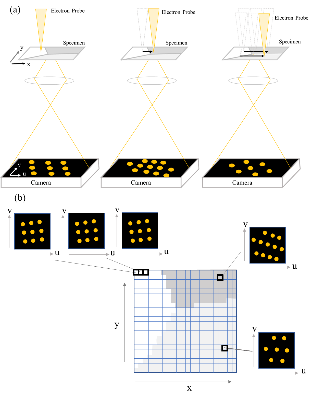
Fig. 1. (a) 4D-STEM data acquisition method: An incident electron beam (probe) is scanned two-dimensionally on a specimen, and at each position, a two-dimensional electron diffraction pattern is recorded using a CCD or CMOS camera. (b) Schematic diagram of a four-dimensional data acquired by the 4D-STEM method.

Fig. 2. Examples of the acquisition conditions of 4D-STEM data; (a) when the convergence angle is small, (b) when the convergence angle is large, and (c) when the camera length is increased to magnify the displacements of the transmitted and diffracted wave disks.
1. Example of orientation analysis of a crystalline specimen
Fig. 3 shows an orientation analysis example of the crystal grains in the vicinity of the grain boundary triple junction of a Mn-Zn ferrite soft magnetic material using 4D-STEM data. The 4D-STEM data was acquired with a small convergence angle to separate the transmitted wave disk and diffracted wave disk as is shown in Fig. 2(a) (For details, see the term “nano-beam diffraction” in Glossary of TEM Terms.).
From the acquired 4D data, four diffraction patterns (Fig. 3(a) right) were extracted from regions A, B, C and D in the annular dark-field STEM (ADF-STEM) image (Fig. 3(a) left). It was found that the crystal orientations at regions A, B and D are different to each other, and that region C is amorphous (halo diffraction pattern of Fig. 3(a) below the middle). This indicates that an amorphous phase is formed near the intersection of the three grains (called “triple junction”).
Furthermore, as is shown in Fig. 3(b), when a specific diffraction spot is selected in the diffraction pattern and the microscope mode is switched to the image mode, the image of the grain with a specific orientation can be displayed. That is, when diffraction spots originating from the crystalline phase (B, D) are selected, the crystal grains B and D orientations are visualized. On the other hand, when the diffuse scattering region C (no diffraction spot) is selected, the amorphous phase is visualized.
Unlike conventional methods, 4D-STEM can reveal the crystal orientation at any position from the acquired 4D data.
2. Example of reconstruction (phase reconstruction) of a crystal structure image using ptychography
Fig. 4 shows an example of reconstructing a crystal structure image (phase image) of a specimen from the acquired 4D-STEM data by ptychography using a high-speed, high-sensitivity camera. The 4D-STEM data was acquired with a large convergence angle to overlap the transmitted wave disk with the diffracted wave disks, as is shown in Fig. 2(b). Fig. 4(a) shows the 3030 and 3030 diffracted wave disks, the reflections being selected from the Fourier-transform of the scanned 2D image or the real space part of the 4D data. The two diffracted wave disks overlap with the 0000 transmitted wave disk. From the overlapping areas, the amplitude and phase of the relevant diffracted wave can be obtained. The phase of the diffracted wave is shown in color and the amplitude in color intensity in Fig. 4(b). The overlapping area between the 3030 diffracted wave disk and the 0000 transmitted wave disk is shown in blue. The overlapping area between the 3030 diffracted wave disk and the 0000 transmitted wave disk is shown in red. The difference of the two colors shows that the phase is shifted byπbetween the two overlapping areas. Note that the intensity in the yellow-green area or outside the black dashed areas A and B is a noise component, so the amplitude is set to zero. Fig. 4(c) shows a crystal structure image (phase image) of the specimen which was reconstructed (inverse Fourier-transformed) using the amplitudes and phases of many reflections obtained from the overlapping areas. This method is called “ptychography”. (See the term “Ptychography” in Glossary of TEM Terms.) In the reconstructed structure image (phase image), not only the Si atoms but also the N atoms are visualized with high contrast.
3. Example of visualizing magnetic domains in a magnetic material
Fig. 5 shows an example of visualizing the magnetic domains in a Mn-Zn ferrite soft magnetic material using 4D-STEM data. The deflection of the transmitted wave disk due to the magnetic moment is used as diffraction data. To observe clearly the deflection (its magnitude and direction) of the electron beam, the diffraction pattern is magnified under a large camera length using the image-forming lens system (Fig, 2(c)).
Fig. 5(a) shows the bright-field STEM (BF-STEM) image of the specimen, which is reproduced from the transmitted wave intensity at each specimen position of the 4D data. By extracting the deflection data of the electron beam (the directions of displacement of the transmitted wave disk) for all pixels of the specimen positions from the 4D data, the magnetic domain structure (Fig. (5b)) was revealed. The arrows shown in Fig. 5(b) indicate the directions of the magnetic moments determined from the directions of the displacements of the transmitted wave disks. In this figure, the directions and the effective magnitudes of the magnetic moments, which were obtained by differential phase contrast imaging*, are additionally shown with different colors and different color intensities, respectively (see color wheel at bottom left). On the right of Fig. 5(b), the transmitted wave disks from three points on the specimen are shown, which were arbitrarily extracted from the 4D data. It is seen that the disks from these points are deflected in different directions due to the differences in the orientations of the magnetic moments (orange cross lines are drawn in the disks to make the deflection easier to see).
It is noted that since the specimen is a soft magnetic material, a closure domain structure (magnetization is closed as a whole) is seen to stabilize the magnetic domains.
*See also the term “differential phase contrast imaging” in Glossary of TEM Terms for reference.
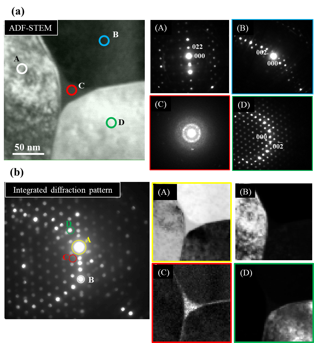
Fig. 3. Example of an orientation analysis of the crystal grains near the grain boundary triple junction of a Mn-Zn ferrite soft magnetic material using 4D-STEM data.
Top (a): The left figure shows an ADF-STEM image. The four figures on the right show the diffraction patterns extracted at specimen points A to D from the 4D data.
Bottom (b): The left figure shows a diffraction pattern, of which intensities were obtained by integrating over the entire specimen. The four figures on the right show STEM images obtained from the diffraction spots A to D:(A) BF-STEM image and (B, C, D) DF-STEM images.
(The result was obtained by the joint research with Zentaro Akase, Associate Professor, Nara Institute of Science and Technology)
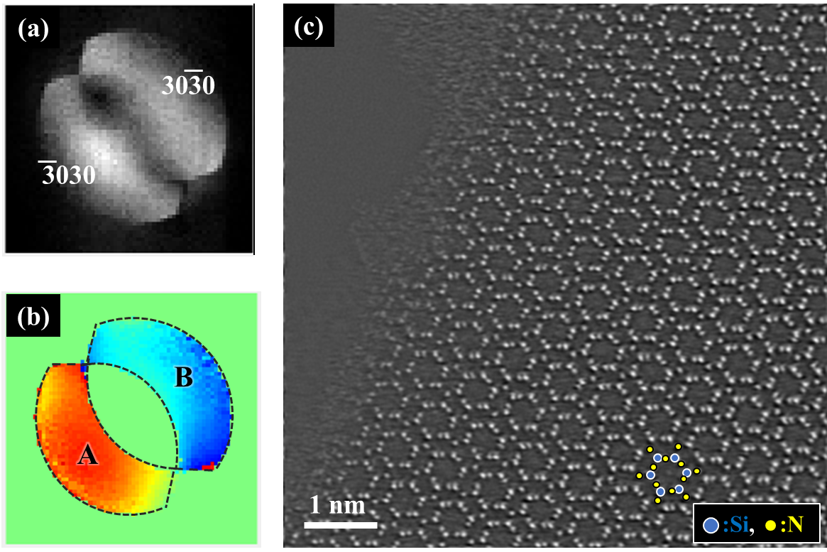
Fig. 4. Example of reconstructing the crystal structure image (phase image) of β-Si3N4 by ptychography using the 4D data. The row data was taken at the [0001] incidence using a Cs-corrected transmission electron microscope at an accelerating voltage of 200 kV. (a) The convergent-beam diffraction patterns of the 3030 and 3030 reflections, the reflections being selected from the Fourier-transform of the scanned 2D image in the 4D data. (b) Blue and red colors indicate that the phase inversion between the two diffracted waves, the phases being opposite between the two disks. (c) Crystal structure image (phase image) reconstructed by ptychography processing.
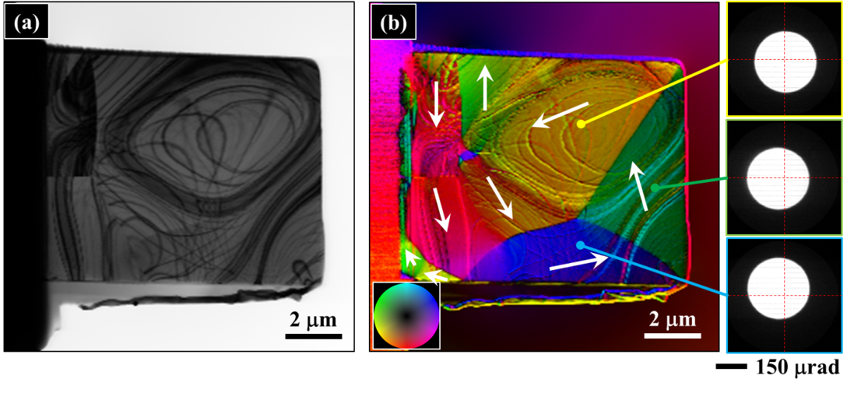
Fig. 5. Example of visualizing the magnetic domains in a Mn-Zn ferrite soft magnetic material by 4D-STEM. (a) BF-STEM image reproduced using the 4D-STEM data. (b) Visualized magnetic domain structure of the specimen (center). Three transmitted wave disks for three points on the specimen extracted from the 4D-data (right), where the electron beam for each point is deflected in a different direction due to the different orientation of the magnetic domain.
Related Term(s)
Term(s) with "4 dimensional-scanning transmission electron microscopy, 4D-STEM" in the description
Are you a medical professional or personnel engaged in medical care?
No
Please be reminded that these pages are not intended to provide the general public with information about the products.