Ptychography
Ptychography
Ptychography is a method to reconstruct the crystal structure (image) of a specimen from the diffraction patterns obtained from each point (area) scanned over a specimen using a convergent probe so that a part of the illuminated area overlaps. "Ptycho" means "fold" in Greek. This method has been used in X-ray crystal structural analysis.
Ptychography for Electron Microscopy has attracted attention as one of methods to obtain the crystal structural image (phase recovery) of atomic resolution since about 2012, owing to the advent of a high-speed and high-sensitivity camera that achieves fast acquisition of a two-dimensional (2D) digital image, together with improvement of microscope stability and advancement of the aberration corrector. In particular, it has been reported in recent electron ptychography studies that low-noise and high-contrast crystal structure images are obtained (Fig. 2), thus gaining increased attention. In transmission electron microscopy, the following two types of ptychography methods are being conducted.
1) Scanning Method Using a Defocused Incident Electron Beam on a Specimen Crystal (Fig. (a))
A specimen is illuminated with a defocused convergent electron probe to broaden the illumination area. The probe is scanned on the specimen so that the adjacent illumination areas are partially overlapped with each other. The scanning points of the probe are typically fewer than several tens × several tens, depending on the scanning area and probe size. The procedure to obtain a crystal structure image (phase image) by means of this type of ptychography is as follows:
The initial specimen function is assumed equal to unity, and the probe function is assumed to be a box function. The exit-wave function from the specimen (the product of the specimen function and probe function) is Fourier-transformed to obtain the diffraction pattern. The amplitudes of the calculated diffraction pattern are replaced by the square root of the experimentally measured intensities, the phases of the diffraction pattern being unchanged. The updated diffraction pattern is inverse Fourier transformed to obtain the real space image (structure image), which gives a new revised specimen function at that probe position. The probe function obtained is replaced with the correct (initially defined) function, and the above procedure is repeated. Then, the same calculation procedure is carried out at the next position. The entire sequence of the procedure is repeated until the difference between the calculated and experimental diffraction patterns becomes sufficiently small [1].
The resulting crystal structural image (phase recovered image) of the specimen is shown in Fig. (c). Although the present method is similar to conventional incoherent diffractive imaging, it should be noted that non-unique solution problem in diffractive imaging is overcome due to the additional constraint, in which the specimen function in the overlapping region of the adjacent illumination areas must be the same. Furthermore, the observation area is no longer limited, as it can be expanded through scanning.
2) Scanning Method Using a Focused Incident Electron Beam on a Specimen Crystal (Fig. (b))
When a convergent electron beam is focused onto the specimen surface, a convergent beam electron diffraction (CBED) pattern - a disk shape pattern - forms on the back focal plane of the objective lens. By scanning this focused electron beam two-dimensionally across the specimen (with the number of scanning points exceeding tens of thousands) and by acquiring CBED patterns at each point, a four-dimensional dataset is obtained that includes images for each incident direction, i.e., (2D scanning image + 2D diffraction pattern).
Next, for the four-dimensional dataset RK composed of [2D scanning image R + 2D diffraction pattern K], a Fourier transform is applied to the scanning image R to obtain a diffraction spot pattern Q. As a result, a new four-dimensional dataset QK is formed, consisting of [2D diffraction spot pattern Q + 2D diffraction pattern K]. By selecting a specific diffraction spot (reflection) q from Q, the interference region (K') between the CBED disk K corresponding to the spot q and the transmitted wave disk contains the amplitude and phase information of the Fourier component q of the crystal structure—assuming the weak phase object approximation holds for the present case (see the lower part of Fig. (b)).
Subsequently, for many diffraction spots (reflections) q, their amplitudes and phases are extracted from the overlapping regions of the CBED patterns (K' and K'' in the lower part of Fig. (b)). By applying the inverse Fourier transform to the modified 2D diffraction spot pattern Q', which reflects the obtained amplitudes and phases, a structural image (phase image) of the specimen crystal is reconstructed (Fig. (d)). This method is expected to improve signal-to-noise (S/N) ratio and contrast better than those obtained with ADF (annular dark-field) imaging [2].
It is noted that in this procedure, the sign (phase) of the amplitude of the interference region (K'') between the diffracted wave (−q), which is symmetrically positioned with respect to the transmitted wave, and the transmitted wave is inverted to the same phase of the amplitude in the interference region (K'). This operation enables the enhancement of signal intensity by adding signals that would normally cancel each other out during integration between regions K' and K''. Furthermore, to improve the signal-to-noise (S/N) ratio of the resulting structural image (phase image), the intensity outside the interference regions (K', K'') is set to zero.
It should be noted that the technique described here is considered to be applicable not only to crystalline materials but also to amorphous substances [3].
(Proofread by: Associate Professor Peng Wang, University of Warwick)
References:
[1]A. M. Maiden and J. M. Rodenberg: Ultramicroscopy, 109 (2009) 1256
[2]T. J. Pennycook et al.: Ultramicroscopy, 151 (2015) 160
[3]C. M. O’Leary et al.: Ultramicroscopy, 221 (2021) 113189
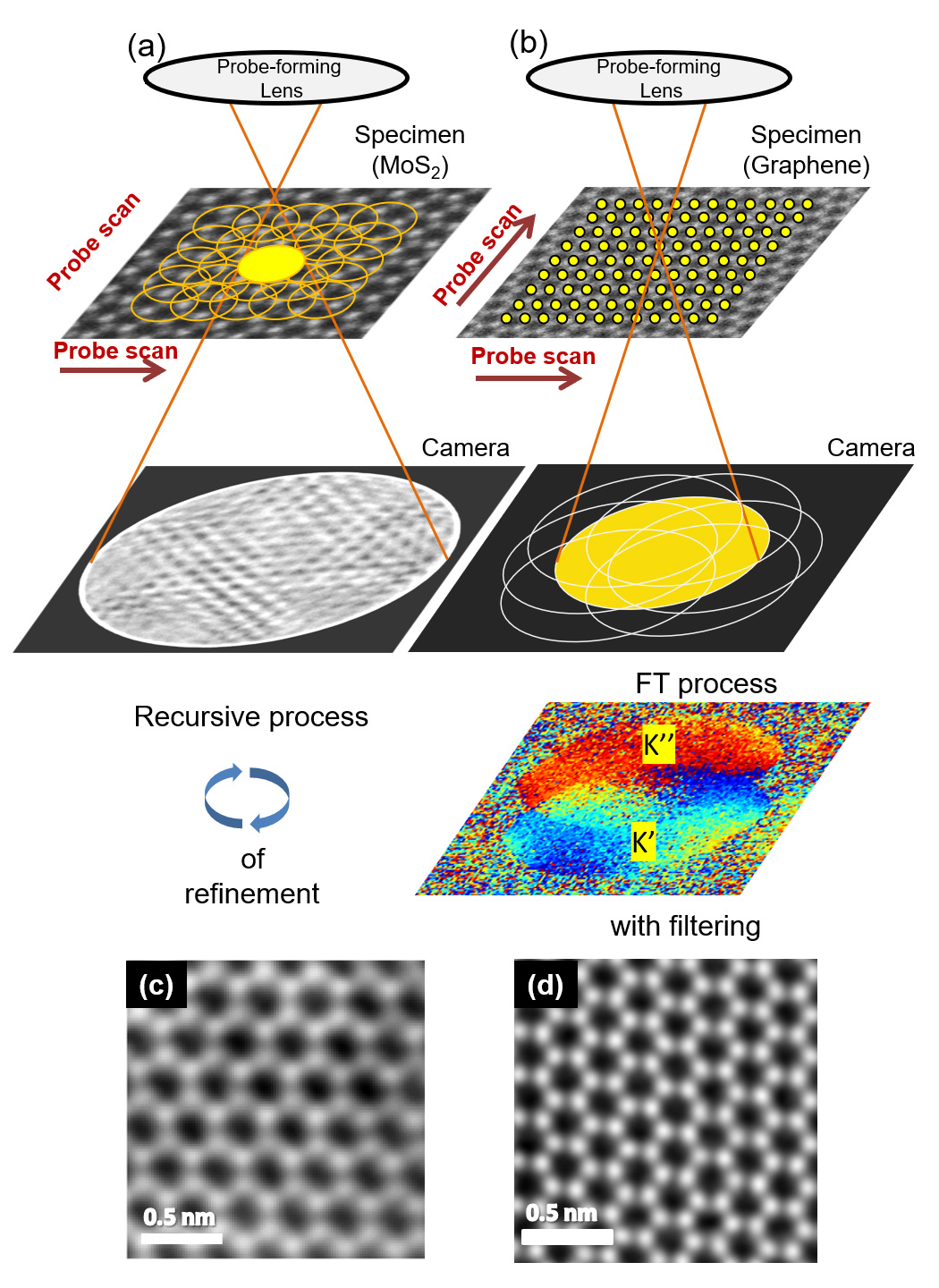
Fig. 1
(a) Ptychography in which a specimen is scanned with a defocused convergent electron probe so that adjacent illumination areas are partially overlapped to each other. The illumination area is about a few nm to a few 10 nm in diameter. The number of the scanning points is normally a few 10 times a few 10 or less.
(b) Ptychography in which a specimen is scanned with a focused convergent electron probe (probe diameter: about 0.3 nm or less). The number of the scanning points is a few 100 times a few 100 (the total number exceeding tens of thousands) like the case of ordinary STEM. A high-speed and high-sensitivity camera (pixel array STEM detector) is used to obtain a series of the CBED patterns.
(c) Structure image (Phase image) of a mono-layer of MoS2 reconstructed by the defocus method (a). (Data courtesy: Associate Professor Peng Wang, University of Warwick)
(d) Structure image (Phase image) of a mono-layer graphene reconstructed by the focus method (b).
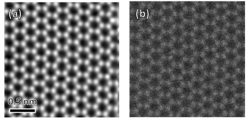
Fig. 2
Comparison of a reconstructed structure image (phase) obtained by Ptychography in which a specimen is scanned with a convergent probe and a simultaneously-obtained ADF image of a mono-layer graphene acquired at an accelerating voltage of 80 kV.
(a) Structure image (phase) of graphene reconstructed from 4D data set. Here, the atomic sites appear bright.
(b) Ordinal ADF image simultaneously acquired with the 4D data set.
Comparison of the two images elucidates that the reconstructed structure image (phase) has a higher signal-to-noise ratio and provides higher contrast than those of the ADF image.
Related Term(s)
Term(s) with "Ptychography" in the description
Are you a medical professional or personnel engaged in medical care?
No
Please be reminded that these pages are not intended to provide the general public with information about the products.