surface plasmon
surface plasmon
When a metal surface or an interface between a metal and a dielectric material (with vacuum) is irradiated by a charged-particle or a light wave, electric charges are induced at the surface or the interface for generating an electric field. With this electric field as a driving force, the charges on the surface or the interface induce longitudinal oscillations. This phenomenon is called "surface plasmon".
[Creation of surface plasmon]
The electric field generated by the surface charges possesses the components parallel and vertical to the surface (Fig. 1(a)). The electric-field component parallel to the surface (Ex) acts as a driving force to induce longitudinal oscillations. On the other hand, the change in time of the electric-field component vertical to the surface (Ez) induces electromagnetic waves along the surface. The longitudinal wave that matches the periodicity of these electromagnetic waves is enhanced and propagates. As a result, a surface plasmon is created. The surface plasmon is abruptly attenuated as the depth from the surface is large. Unlike the volume plasmon, the surface plasmon is observed with not only an electron wave but also a light wave. This is due to the fact that, the electric field vertical to the surface corresponds to the transverse wave component against the surface plasmon, and the external electromagnetic waves interact with the transverse wave component.
[Equations of surface plasmon]
For the interface between a metal and a dielectric material, the electric-field components vertical to the metal side and the dielectric material side are expressed as Ez=0- 、Ez=0+, respectively. Since the electric flux densities of the metal side and the dielectric material side are equal, εMEz=0-=εdEz=0+ is given. Here, εM and εd are the dielectric constant for metal and that for dielectric material, respectively. As shown in Fig, 1(b), -Ez=0-=Ez=0+, and thus
・・・(1)
is obtained. Then, the dielectric constant for metal εM is replaced by the dielectric function εM (ω)=1-(ω_P/ω)2 based on the free electron model. Here, is the angular frequency of the surface plasmon. When the equation (1) is solved for ω, the surface plasmon energy ES is given by the following equation.
・・・(2)
Here, EP=ћωP corresponds to the volume plasmon energy. The surface plasmon energy of the interface between a metal and a vacuum is because the dielectric constant of the vacuum is εd=1.
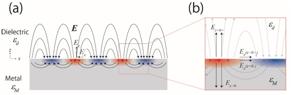
Fig. 1 (a) Schematic of surface plasmon for metal. Due to an external charged-particle or a light wave, the positive (+) and the negative (–) charges are induced. With an electric field generated by these charges (Ex (z=0±) in Fig. 1) as a driving force, a longitudinal oscillation wave of free electrons is created. (b) Illustration of the electric-field component vertical to the interface between a metal and a dielectric material (with vacuum) Ez=0± and the electric-field component parallel to this interface Ex (z=±0). Both of the continuity for the vertical component of the electric flux density εMEz=0-= εdEz=0+ and the continuity of the parallel component of the electric field are satisfied.
[Experimentally-obtained surface plasmon]
Fig. 2 shows a spectrum of aluminum (Al) acquired by electron-energy loss spectroscopy (EELS). In general, the surface of Al is coated by an oxide film. A spectral peak at 15 eV is due to the volume plasmon. A peak at 7 eV created by the surface plasmon is also seen. Since the dielectric constant of an Al oxide film (Al2O3) is εd=3.7, the surface plasmon energy is calculated to be ES=6.9 eV, which shows a good agreement with an experimental value.
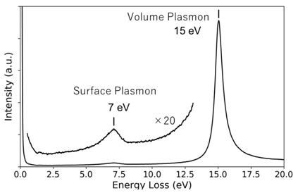
Fig. 2 EELS spectrum of Al. A peak at 15 eV is due to the volume plasmon. A peak at 7 eV is created by the surface plasmon which originates from the interface between Al and an Al oxide.
In metals containing d electrons (Ag, Au, etc.), the interband transitions of d electrons takes place at an energy position which is very close to that of the expected surface plasmon energy, and the surface plasmon strongly interacts with the interband transition. Thus, the aforementioned equation (2) is not applicable and the surface plasmon is seen at a lower energy side compared to the value calculated in the equation (2). In semiconductors like silicon (Si) and GaAs, the surface plasmon is observed at the energy position that is the same as the energy calculated in the equation (2). However, the surface plasmon loses its energy due to the interband transition, leading to the oscillation attenuation and a resultant broad spectral peak. In insulators (diamond, ion crystal, etc.) where valence electrons are strongly bounded, the spectral peak due to the interband transition dominates strongly in an EELS spectrum and thus, the surface plamson appears as a weak background for making its observation difficult.
It should be noted that, a surface plasmon is excited at the surface of a very small metallic particle or a metallic wire with its size being the nanometer-order. In this case, a compressional wave of the surface charge is induced as a characteristic oscillation mode (standing wave) which depends on the shape of the very small particle or the wire. Since this wave is confined in the very small particle, this phenomenon is called "localized plasmon".
(By Associate Professor Yohei Sato, Tohoku University)
Related Term(s)
Term(s) with "surface plasmon" in the description
Are you a medical professional or personnel engaged in medical care?
No
Please be reminded that these pages are not intended to provide the general public with information about the products.