electron energy-loss spectroscopy, EELS
electron energy-loss spectroscopy
When the incident electrons pass through a substance, certain electrons are scattered and lose a part of their energies (traveling speed becomes slow) by the Coulomb interactions with the electrons and the atomic nuclei in the substance. These electrons are called inelastically scattered electrons. The spectroscopic method to obtain energy-loss spectra of inelastically scattered electrons is named "electron energy-loss spectroscopy (EELS)."
Combined with transmission electron microscopy (TEM), EELS enables qualitative and quantitative analysis of the constituent elements and measurement of the dielectric properties (bonding states of the electrons) from a micro- or nano-scale specimen (substance) area. Elementary processes of inelastic scattering analyzed by EELS are: (1) excitations of lattice vibrations (a few 10 to a few 100 meV), (2) interband transitions due to valence electron excitations (0 to 10 eV), (3) plasmon excitations due to collective oscillations of free electrons and valence electrons (10 to 50 eV), and (4) inner-shell excitations or core excitations (50 eV or higher).
Energy loss function and dielectric function
The intensity distribution of an energy-loss spectrum is given by the loss function Im[-1⁄ε(ω)], where ε(ω) is the dielectric function, which is a function of the angular frequency ω of an external electric field [1]. (The angular frequency ω is related to the energy loss ELoss of the electron beam by ħω=ELoss.) The dielectric function is the dielectric response of a substance to the external electric field with angular frequency ω, or expresses the dielectric properties of the substance. The loss function is expressed in the following equation using the real part ε1(ω) and the imaginary part ε2(ω) of the dielectric function.
When an external oscillating electric field is applied to the substances, the center of gravity of the valence electrons is displaced from the atomic nucleus and then the electron polarization  is induced. Here, N is the number of atoms in a unit cell, V is the volume of a unit cell, q is the electric charge of the valence electrons, and r (ω) is the displacement vector of the valence electrons. The dielectric function is expressed using electron polarization P(ω) as
That is, dielectric function ε(ω) is determined by the electron polarization P(ω). The attenuation of polarized oscillations of the valence electrons is expressed by the imaginary part of P(ω), and thus the energy-loss corresponds to the imaginary part of ε(ω).
Valence-loss spectra
The EELS spectrum in a low energy region (0 to 50 eV) is called the valence-loss spectrum. This energy region corresponds to the dielectric response for the frequency ω = ~1015 Hz (E = 10 to 20 eV), where the valence electrons cause resonant oscillations. ε1(ω) exhibits a spectral distribution specific to a resonant state (Fig. 1(b)). When the value of ε2(ω) is small and ε1(ω) is 0 (zero) or very small, the loss function (1) shows a sharp peak. This frequency ω is called the plasma frequency ωp, and the energy of the plasma oscillation is expressed as E=ħωp.
When an electron beam (or a charged-particle beam) is incident on a substance, the Coulomb interaction of the whole of free electrons or valence electrons in the substance with the incident electron induces a charge-density oscillation or a longitudinal wave oscillation of the electrons of the substance. The longitudinal wave oscillation is called plasmon. On the other hand, when a light wave or an electromagnetic wave is incident on the substance, the plasmon of longitudinal wave oscillation cannot be excited because the light is a transverse wave oscillation. Furthermore, the plasmon cannot be observed by the light wave. An optical absorption spectrum expresses the energy absorption due to the attenuation of the dipole oscillation of valence electrons and the spectrum is proportional to the imaginary part ε2(ω) of the dielectric function.
Fig. 1(a) shows an energy loss spectrum due to valence electron excitations of graphite. Fig. 1(b) shows the real part ε1(ω) (blue line) and the imaginary part ε2(ω) (red line) of the dielectric function of graphite. A spectral peak at 27 eV in Fig. 1(a) is due to the collective longitudinal oscillation of the valence electrons (total of the π electrons and the σ electrons) of graphite, the oscillation being called the π+σ plasmon. A spectral peak at 6.5 eV in Fig. 1(a) is originated from the π-π* interband transition and is called the π plasmon. It is seen in Fig. 1(b) that the plasmon excitation condition ε1(ω) = 0 is satisfied at 6.5 eV and 27 eV (shown with black points).
The real part ε1(ω) of the dielectric function shows the resonance-type dispersion respectively due to the π-π* interband transition at 4.2 eV and due to the σ-σ* interband transition at 11.7 eV. Thereby energy absorption due to the interband transitions or the emergence of a spectral peak of the imaginary part ε2(ω) of the dielectric function takes place. It should be noted that the peaks of ε2(ω) due to the transitions cannot be observed in the loss function (Fig. 1(a)). To obtain the dielectric function ε(ω) representing the characteristic feature of a substance from the loss function, it is needed to apply the Kramers-Kronig transform to the loss function [2]. The dielectric function ε(ω) obtained by the transform can be compared with the results of the optical measurements such as the reflectance, the refractive index, the photo-conductivity.
It should be noted that the spectra experimentally obtained contain the multiple scatterings due to the plasmon. The multiple scatterings are observed at the positions of integral multiples of the plasmon energy. As the specimen thickness increases, their intensities increase. To obtain the dielectric function ε(ω), the spectral intensity of single scattering is needed. The spectral intensity of single scattering can be derived from the spectral intensity experimentally obtained by applying the Fourier-log deconvolution method [2]. The method is based upon the fact that the intensities of n-times inelastic scatterings obey the Poisson distribution and their energy distribution is expressed as n-times convolution of the spectral intensity of single inelastic scattering.
The intensity around 0 eV (zero-loss peak) appearing in the energy-loss spectrum is the contribution of elastically scattered electrons. The zero-loss peak has to be carefully subtracted from the measured spectrum because how to subtract the zero-loss peak contributes greatly to the accuracy of spectroscopic analysis.
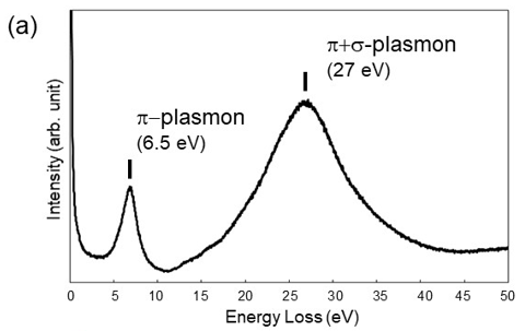

Fig. 1(a) Energy loss spectrum due to valence electron excitations of graphite. A spectral peak at 6.5 eV corresponds to the π plasmon and a spectral peak at 27 eV to the π+σ plasmon. (b) The real part ε1(ω) (blue line) and the imaginary part ε2(ω) (red line) of the dielectric function of graphite. In (b), two black points at 6.5 eV and 27 eV show ε1(ω)=0, indicating the plasmon excitation condition. They correspond to two spectral peaks in the EELS spectrum (a). The peaks of ε2(ω) at 4.2 eV and 11.7 eV in (b) exhibit respectively the energy absorption due to the π-π* interband transition and due to the σ–σ* interband transition. It should be noted that these peaks cannot be observed in EELS spectra, as seen in (a).
Core-loss spectra
The EELS spectrum in the high energy region (50 eV or higher) is called the core-loss spectrum. Since the angular frequency ω(1016 Hz or higher) in this energy region is high, the valence electrons cannot follow the frequency ω and then the polarization becomes small or ε1(ω) ~1. The absorption also becomes sufficiently small and then ε2(ω)≪1. As a result, the loss function can be approximated to be
Thus, the loss function in this case gives the same physical quantity as the absorption spectrum (ε2(ω)) of light (X-ray). The energy loss in this energy region corresponds to the energy absorption where the core electron is excited to the conduction band. From the energy values of the absorption spectra, qualitative and quantitative analyses of the constituent elements in the specimen can be performed. From the spectral intensity distribution, the density of states (DOS) of the conduction band and the bonding states of the electrons in the specimen can be investigated.
Bonding states of electrons in carbon materials and their core-loss spectra
Fig. 2(a) shows the schematic of the electronic states of graphite and of diamond. Carbon atoms in graphite form the σ bond due to the sp2 hybrid orbital and the π bond due to the pz orbitals. The valence band of graphite is created by the σ bonding orbitals (σ orbital) and the π bonding orbitals (π orbital). The conduction band is created by the π anti-bonding orbitals (π* orbital) and the σ anti-bonding orbitals (σ* orbital). The valence band due to the π orbitals overlaps slightly with the conduction band due to the π* orbitals, creating a half-metal.
Carbon atoms in diamond form the σ bond due to the sp3 hybrid orbital but does not form the π bond. The valence band of diamond is created by the σ orbitals. The conduction band is created by the σ* orbitals. A band gap with 5.5 eV exists between these two bands. Fig. 2(b) shows a core-loss spectrum of graphite. A spectral peak at 285.5 eV corresponds to the transition from the 1s orbital to the conduction band formed by the π* orbitals. Spectral intensities from 292 to 310 eV correspond to the transitions from the 1s orbital to the conduction band formed by the σ* orbitals. Since the valence band created by the π orbitals and the σ orbitals is already occupied by the electrons, the transition from the 1s orbital to the valence band cannot occur. A sharp peak at 291.5 eV (▼) is attributed to the exciton, which is a bound state of a hole created in the 1s orbital and an electron excited to the σ* orbital by the Coulomb force.
Fig. 2(c) shows a core-loss spectrum of diamond. The intensity distribution corresponds to the transitions from the 1s orbital to the conduction band formed by the σ* orbitals. Since diamond does not have the π orbitals and the π* orbitals, the spectral peak around 285 eV does not appear. A sharp peak at 289 eV (▼) is attributed to the exciton, where a hole created in the 1s orbital and an electron excited to the σ* orbital are bound to each other by the Coulomb force. Since the π bond does not exist but the band gap exists in diamond, the onset energy of the spectral intensity of diamond (at 288 eV) is a little higher than the onset energy of graphite (at 284 eV).
Thus, the core-loss spectrum reveals the bonding states of the electrons or the states of the π* bond and the σ* bond. The intensity distribution in the spectrum is closely related to the state density of the conduction band or the electronic structure of the anti-bonding orbitals. It should be noted that EELS cannot observe the electronic structure of the valence band (occupied states).

Fig. 2 (a) Schematic of the electronic structures of graphite and diamond, and their electron transition processes from the 1s orbital to the 2p conduction band.
In graphite (left figure), its valence band (blue) is composed of the π orbitals and the σ orbitals, and its conduction band is composed of the π* orbitals and the σ* orbitals.
In diamond (right figure), its valence band (blue) is composed of the σ orbitals, and its conduction band is composed of the σ* orbitals.
Red dotted lines indicate the exciton level of graphite and diamond, which is a bound state between a hole created in the 1s orbital and an excited electron by the Coulomb force.
(b) Core-loss spectrum of graphite. A spectral peak at 285.5 eV corresponds to the transition from the 1s orbital to the π* conduction band. The spectral intensities between 292 eV and 310 eV correspond to the transitions from the 1s orbital to the σ* conduction band. A sharp peak at 291.5 eV (▼) corresponds to the transition from the 1s orbital to the exciton level.
(c) Core-loss spectrum of diamond. The spectral intensities from 288 eV to 310 eV correspond to the transitions from the 1s orbital to the σ* conduction band. A sharp peak at 289 eV (▼) corresponds to the transition from the 1s orbital to the exciton level.
Comparison between EELS and XES
EELS is a method to investigate the electronic structure of the conduction band (unoccupied states), but cannot obtain that of the valence band (occupied states). The electronic structure of the valence band can be investigated by X-ray emission spectroscopy (XES), which is a spectroscopic method to measure the X-ray emission spectrum generated by irradiating a specimen with an electron beam. That is, when the electron beam is incident on the specimen, the electron in an inner shell is emitted and a hole is created there. Then, an electron of the valence band falls to the hole and X-ray emission occurs at this transition. The XES spectrum acquired enables us to obtain the density of states (DOS) of the valence band. Combined analysis with EELS and XES provides the electronic structures of both the conduction band (unoccupied states) and the valence band (occupied states).
Current status of EELS instruments
High energy-resolution EELS measurement is performed using a TEM equipped with a monochromator to monochromatize the energy of the incident electron beam and with an energy analyzer to obtain spectra of inelastically scattered electrons. When a TEM equipped with a monochromator of commercial type is used at an accelerating voltage of 200 kV, EELS spectra with an energy-resolution of 0.2 eV or better can be acquired. Nowadays, the TEMs incorporating a monochromator which enables superbly high energy-resolution are being developed. Some instruments have achieved a few meV energy resolution. With an improved energy resolution, the measurable energy region by EELS has extended to the infrared region (a few meV to 0.5 eV), thus enabling spectroscopic analysis of inelastically scattered electrons due to lattice vibrations (a few 10 to a few 100 meV), which have been treated as quasi-elastically scattered electrons. Taking advantage of such high performance, measurements of lattice and molecular vibrations in local areas have been conducted by EELS.
Momentum transfer resolved EELS (q-EELS)
Inelastically scattered electrons give a momentum q to the electrons in a substance and are scattered in the direction -q against the incident-beam. A method to obtain the energy loss spectra of the inelastically scattered electrons as a function of momentum transfer q, rather than to obtain simply energy loss spectra, is called the momentum transfer resolved EELS (angle resolved EELS or q-EELS) method.
The electron transition by a light beam causes only the transition of q ~0, but the electron excitation by an electron beam allows the transitions of q ≠ 0. Thus, when an electron beam is incident on a substance, the dielectric function ε(q,ω) which takes account of the q dependence of the dielectric function can be obtained from the analysis of the q dependent valence-loss spectra. Measurement of the q dependent core-loss spectra reveals the q dependence of DOS of the conduction band and the orientation of the anti-bonding orbitals (unoccupied states).
References
[1] H. Raether, Springer Tracts in Modern Physics, 88 (1980), Excitation of Plasmons and Interband Transitions by Electrons (Springer-Verlag Berlin Heidelberg GmbH, 1980)
[2] R.F. Egerton, Electron Energy-Loss Spectroscopy in the Electron Microscope, Third Edition (Springer, 2011)
(By Associate Professor Yohei Sato, Tohoku University)
Related Term(s)
Term(s) with "electron energy-loss spectroscopy" in the description
Are you a medical professional or personnel engaged in medical care?
No
Please be reminded that these pages are not intended to provide the general public with information about the products.