dislocation
dislocation
"Dislocation" is a linear or one dimensional defect in a crystal. When a part in a crystal is displaced against the other part, the line at which the displacement is starting is called a dislocation or a dislocation line. There are two types of dislocations, or edge dislocations and screw dislocations. The crystal around the dislocation is highly strained. Plasticity of a crystal is explained by motion and multiplication of dislocations.
Fig. 1(a) schematically shows the atomic arrangement near an edge dislocation of a cubic crystal. An extra lattice plane (called an extra half plane) is shown by a black line. The end line of the extra half plane is the edge dislocation or edge dislocation line. Suppose a circuit along the crystal lattice around the dislocation line (Burgers circuit: indicated by yellow lines with allows), the end of the circuit after one round does not come back to the original lattice point but comes to the next lattice point. This displacement is termed the Burgers vector (indicated by a red allow), which characterizes the direction and amount of the atomic displacement caused by the dislocation. The Burgers vector (shown by a red line) of the edge dislocation is perpendicular to the dislocation line.
Fig. 1(b) schematically shows the atomic arrangement near a screw dislocation. The screw dislocation (line) exists at the start (or end) line of the displacement and runs from the top to the bottom of the figure. The Burgers circuit in this case is seen to be spiral. The Burgers vector of the screw dislocation is parallel to the dislocation line (indicated by a red allow).
Fig. 2 shows a bright-field image of dislocations in a silicon crystal. The dislocations (lines) are seen to be dark (black) lines because the regions near the dislocations come into a Bragg reflection. Fig. 3 shows a [001] atomic-resolution dark-field STEM image of a small-angle grain boundary of SrTiO3. Edge dislocations are seen to be arranged along the grain boundary, creating a small orientation change between both sides of the crystal.
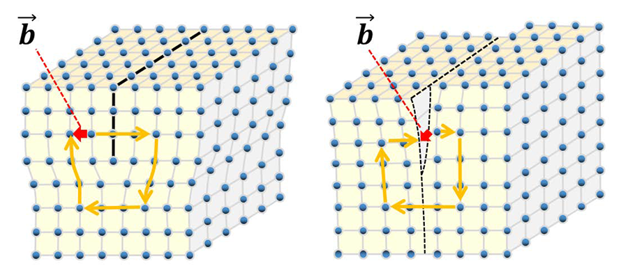
Fig. 1.(a) Schematic of edge dislocation. (b) Schematic of screw dislocation.
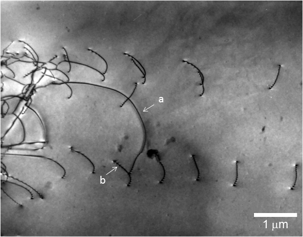
Fig. 2. Bright-field image of dislocations in a silicon crystal taken at an accelerating voltage of 200 kV.
(a) A black line (indicated by arrow "a") shows a dislocation line running parallel to the specimen surface.
(b) A black zigzag line (indicated by arrow "b") exhibits a dislocation running oblique to the specimen surface. The zigzag contrast is created by a dynamical diffraction effect.
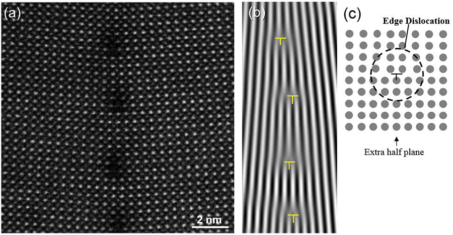
Fig. 3
(a) [001] atomic-resolution dark-field STEM image of dislocations on a small-angle grain boundary of SrTiO3 taken at an accelerating voltage of 200 kV. (Specimen courtesy: Prof. Y. Ikuhara, The University of Tokyo)
(b) Edge dislocations are clearly visualized by selectively displaying crystalline planes along the grain boundary.
(c) Schematic of the edge dislocation (gray circles indicate atomic columns).
Related Term(s)
Term(s) with "dislocation" in the description
Are you a medical professional or personnel engaged in medical care?
No
Please be reminded that these pages are not intended to provide the general public with information about the products.