scanning electron microscope, SEM
scanning electron microscope
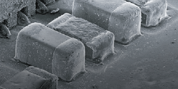
An electron microscope in which a small electron probe is scanned over the surface of a bulk specimen, and secondary or backscattered electrons emitted from the surface are collected by a detector, and finally, the intensity of the detected signal is displayed on a computer monitor screen as a series of bright spots synchronized with the scan of the electron probe. An image formed by secondary electrons enables us to observe the fine structure or morphology of the surface of the bulk specimen, whereas an image formed by backscattered electrons provides the difference in the composition of the specimen. The "scanning electron microscope (SEM)" is used by adding various analytical functions (tools) such as EDS and WDS. An important factor that determines the SEM resolution is the size of the incident electron probe (beam) on the specimen. To decrease the probe size, the most essential point is to decrease the size of the electron (emission) source. The cold cathode FEG has the smallest source size, followed by the Schottky FEG, the LaB6 (tip) electron gun, and the tungsten (filament) electron gun. The second most essential point that determines the probe size is the selection of the objective lens. Three types of objective lenses are available; (1) out-lens type, (2) snorkel lens type, and (3) in-lens type. In the out-lens type, a specimen is placed below the objective lens allowing tilting a large specimen. In this lens, limitation on specimen size is not severe but the production of a small beam is difficult because the focal length of the lens becomes large. In the in-lens type, a specimen is inserted into the objective lens in the same manner as the TEM. In this lens, a small probe can be produced because the focal length can be made small. However, the specimen size is limited to several mm. The snorkel lens has a compromise design between the out-lens and in-lens. (The term, "snorkel," originates from the fact that the lens geometry resembles a snorkel used by divers.) A specimen is placed below (not far from) the objective lens. Thus, a relatively small probe can be produced and also a relatively large specimen can be treated. The SEM resolution is degraded at low accelerating voltages due to the chromatic aberration effect. Normally, the resolution is defined at 20 to 30 kV. An ultra-high resolution SEM achieves a resolution of about 1 nm, whereas a general-purpose SEM provides a resolution of about 10 nm. The use of a Cs corrector or a Cc corrector enables a further decrease of the incident-beam size, but causes a disadvantage of a short focal depth because the acceptance angle becomes larger. As the accelerating voltage of the incident electrons is decreased, the penetration depth of the electrons becomes smaller. This reduces a spread of secondary electrons generated by backscattered electrons in the specimen, thus enhancing the image contrast. Advantages of low accelerating voltage include the reduction of the background in the image, the decrease of charging, and the decrease of damage to the specimen. In SEM, charging degrades the image quality. If the current of the incident electrons exceeds the current of electrons flowing out of the specimen, charging takes place. The charging disturbs the image, sometime forming nothing like the true image. When a nonconductive specimen is used, to prevent charging, the specimen is coated with a conductive material, such as noble metal, Al and C. In a low-vacuum SEM, a nonconductive specimen may be observed without coating.
Related Term(s)
Term(s) with "scanning electron microscope" in the description
Are you a medical professional or personnel engaged in medical care?
No
Please be reminded that these pages are not intended to provide the general public with information about the products.