convergent-beam electron diffraction, CBED
convergent-beam electron diffraction
A method for qualitative and quantitative analysis of crystal structures from a disk diffraction pattern, acquired by illumination of a cone-shaped convergent electron beam on a small specimen area with a diameter of 10 nm or less. The CBED disk displays the intensity distribution corresponding to changes of diffraction conditions (rocking curve). The method enables us to determine not only specimen thickness, lattice parameter, crystal symmetry (point group and space group) and characteristics of a lattice defect, but also a crystal structure (refinement of atomic coordinates, Debye-Waller factors, low-order structure factors (potential distribution)). When the large-angle convergent-beam electron diffraction (LACBED) technique is applied, the characteristic feature of a lattice defect is easily and unambiguously identified and the strains (and a dislocation) at interfaces of a multi-layer material are determined with a high accuracy. The use of an energy filter allows us to conduct more accurate structure analysis.
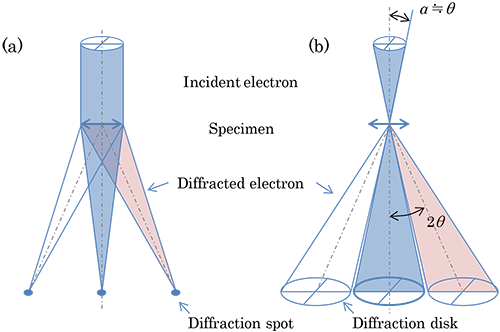
(a) Conventional electron diffraction (Selected-area diffraction)
Illuminating a parallel electron beam onto a specimen forms a spot diffraction pattern on the back focal plane of the objective lens. This diffraction pattern is magnified with the imaging lens system and then displayed on a screen. In the figure, the ray path with the imaging lens system is omitted.
(b) Convergent-beam electron diffraction
Illuminating a cone-shaped electron beam onto a specimen forms a disk diffraction pattern on the back focal plane of the objective lens. This diffraction pattern is magnified with the imaging lens system and then displayed on a screen.
In conventional CBED, the convergence semi-angle a is limited at the maximum to the Bragg angle q to avoid the overlap of adjacent diffraction disks.
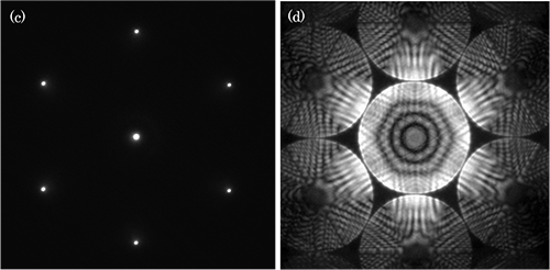
(c) Example of Conventional electron diffraction (Selected-area diffraction) pattern.
Diffraction pattern of Si [111] taken at an accelerating voltage of 200 kV.
(d) Example of Convergent-beam electron diffraction pattern.
CBED pattern of Si [111] taken at an accelerating voltage of 200 kV by eliminating energy loss electrons (Zero-loss pattern).
(a) Conventional electron diffraction (Selected-area diffraction)
Illuminating a parallel electron beam onto a specimen forms a spot diffraction pattern on the back focal plane of the objective lens. This diffraction pattern is magnified with the imaging lens system and then displayed on a screen. In the figure, the ray path with the imaging lens system is omitted.
(b) Convergent-beam electron diffraction
Illuminating a cone-shaped electron beam onto a specimen forms a disk diffraction pattern on the back focal plane of the objective lens. This diffraction pattern is magnified with the imaging lens system and then displayed on a screen.
In conventional CBED, the convergence semi-angle a is limited at the maximum to the Bragg angle q to avoid the overlap of adjacent diffraction disks.
(c) Example of Conventional electron diffraction (Selected-area diffraction) pattern.
Diffraction pattern of Si [111] taken at an accelerating voltage of 200 kV.
(d) Example of Convergent-beam electron diffraction pattern.
CBED pattern of Si [111] taken at an accelerating voltage of 200 kV by eliminating energy loss electrons (Zero-loss pattern).
Related Term(s)
Term(s) with "convergent-beam electron diffraction" in the description
Are you a medical professional or personnel engaged in medical care?
No
Please be reminded that these pages are not intended to provide the general public with information about the products.