annular bright-field scanning transmission electron microscopy, ABF-STEM
annular bright-field scanning transmission electron microscopy
Annular bright-field scanning transmission electron microscopy (ABF-STEM) is a bright-field high-resolution STEM method which preferentially receives only the ring-shaped circumference (e.g. 12 to 24 mrad) of the direct (transmitted)-beam disk using an annular bright-field (ABF) detector, without using the central part of the bright field disk. The integrated intensities of the received electrons are displayed in synchronism with the incident probe position for acquisition of a high-resolution atomic image. The ABF method enables us to effectively visualize atomic columns composed of light atoms.
In these light-element atomic columns, the intensities of electrons which travel along the atomic columns parallel to the incident beam, become higher than the scattered electrons due to the electron channeling effect. Thus, the electrons which are incident on the light atomic columns increase to pass through the center hole of the ABF detector. As a result, light elements are effectively imaged as dark spots (image formed by smaller quantity of electrons). On the other hand, the electrons which are incident on the heavy atomic columns increase to scatter at high angles outside of the ABF detector. As a result, heavy atomic columns are also imaged as dark spots. Thus, the ABF method enables us to observe both the atomic columns of relatively heavy elements (transition metals, etc.) and light elements (O, Li, etc.) with the same contrast.
HREM and BF-STEM have long been used to visualize atomic columns. However, those two methods necessitate image simulations for correct image interpretation because the intensity of the atomic column largely depends on the defocus amount and specimen thickness. In the ABF-STEM image, (except for extremely thin specimen) the atoms are always imaged as dark spots irrespective of the variation of specimen thickness. Even in the image formed with a certain defocus, atoms are still imaged as dark spots because the incident electrons over a certain angular range reduce the interference effect of each electron. This makes an easy interpretation of the ABF image compared to the HREM and BF-STEM images.
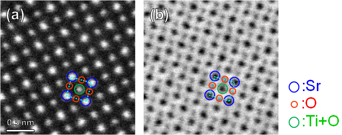
High-resolution STEM images of SrTiO3 taken at the [100] incidence. (Accelerating voltage: 200 kV, Convergence semi-angle of the incident electron beam: 22 mrad)
Fig.(a) HAADF-STEM image taken with an acceptance semi-angle of the detector 90 to 170 mrad. Sr columns and Ti + O columns, which are composed of relatively heavy atoms, are clearly visualized. However, the light-atom O columns cannot be observed as bright spots.
Fig.(b) ABF-STEM image taken with an acceptance semi-angle of the detector 11 to 22 mrad.
The light-atom O columns, which cannot be seen in the HAADF image, are clearly observed as dark spots.
Comparison of Ray diagrams of two detectors
In these light-element atomic columns, the intensities of electrons which travel along the atomic columns parallel to the incident beam, become higher than the scattered electrons due to the electron channeling effect. Thus, the electrons which are incident on the light atomic columns increase to pass through the center hole of the ABF detector. As a result, light elements are effectively imaged as dark spots (image formed by smaller quantity of electrons). On the other hand, the electrons which are incident on the heavy atomic columns increase to scatter at high angles outside of the ABF detector. As a result, heavy atomic columns are also imaged as dark spots. Thus, the ABF method enables us to observe both the atomic columns of relatively heavy elements (transition metals, etc.) and light elements (O, Li, etc.) with the same contrast.
HREM and BF-STEM have long been used to visualize atomic columns. However, those two methods necessitate image simulations for correct image interpretation because the intensity of the atomic column largely depends on the defocus amount and specimen thickness. In the ABF-STEM image, (except for extremely thin specimen) the atoms are always imaged as dark spots irrespective of the variation of specimen thickness. Even in the image formed with a certain defocus, atoms are still imaged as dark spots because the incident electrons over a certain angular range reduce the interference effect of each electron. This makes an easy interpretation of the ABF image compared to the HREM and BF-STEM images.
High-resolution STEM images of SrTiO3 taken at the [100] incidence. (Accelerating voltage: 200 kV, Convergence semi-angle of the incident electron beam: 22 mrad)
Fig.(a) HAADF-STEM image taken with an acceptance semi-angle of the detector 90 to 170 mrad. Sr columns and Ti + O columns, which are composed of relatively heavy atoms, are clearly visualized. However, the light-atom O columns cannot be observed as bright spots.
Fig.(b) ABF-STEM image taken with an acceptance semi-angle of the detector 11 to 22 mrad.
The light-atom O columns, which cannot be seen in the HAADF image, are clearly observed as dark spots.
Comparison of Ray diagrams of two detectors
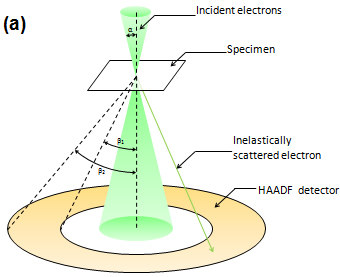 Fig.(a) Relationship between the convergence semi-angle of the incident electron beam and acceptance semi-angles of the detector for HAADF-STEM. Typical inner and outer semi-angles of the detector are respectively β1 = ~50 mrad and β2 = ~200 mrad, detecting inelastically scattered electrons at high angles. The value of the convergence semi-angle α is approximately 25 mrad for a 200 kV Cs-corrected TEM. Usually, an ABF detector and a LAADF detector are placed below a HAADF detector. |
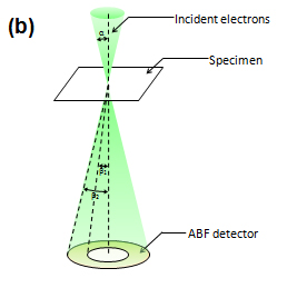 Fig.(b) Relationship between the convergence semi-angle of the incident electron beam and acceptance semi-angles of the detector for ABF-STEM. The inner and outer acceptance semi-angles of the detector are respectively taken as β1 ≒ α/2 and β2 ≒ α, where a is the convergence semi-angle. It should be noted that the only peripheral part of the bright field disk (without the central part) is used for ABF-STEM. In the case of a 200 kV Cs-corrected TEM, α, β1 and β2 are respectively ~25 mrad, ~13 mrad and ~25 mrad. |
Related Term(s)
Term(s) with "annular bright-field scanning transmission electron microscopy" in the description
Are you a medical professional or personnel engaged in medical care?
No
Please be reminded that these pages are not intended to provide the general public with information about the products.