

Semiconductor
Semiconductors are materials whose electrical conductivity lies between that of conductors (which readily allow the flow of electricity) and insulators (which resist the flow of electricity). Integrated circuits composed of numerous transistors and diodes, fabricated from semiconductor materials, are commonly referred to as semiconductors or semiconductor chips. Semiconductors are widely utilized in a broad range of applications, from home appliances and automobiles to critical social infrastructure.
Within the field of semiconductors, new materials such as SiC and GaN, advanced transistor structures, and cutting-edge 3D packaging technologies are receiving a significant attention for achieving lower power consumption and higher performance. To ensure high manufacturing yield and device reliability, precise characterization techniques and the appropriate selection of preprocessing and analytical instruments are essential. This page introduces various analytical instruments and application examples, highlighting their use in semiconductor manufacturing and research.
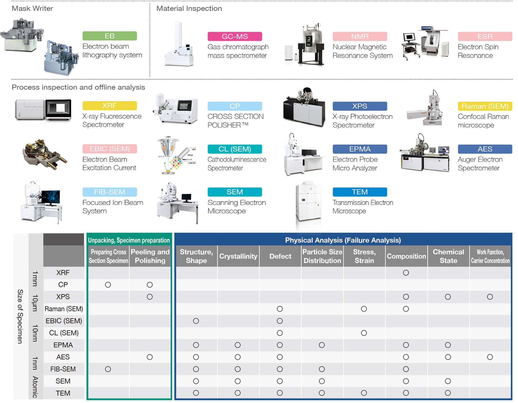
- JEOL's Instruments Contributing to Semiconductor Inspection and Analysis
- JEOL Semiconductor-Related Products and Their Applications
- EB:Electron Beam Lithography System
- FIB-SEM/TEM:Application of TEM-Based CD Measurement in Advanced Semiconductor Processes
- SEM:SEM Functions for Observing and Analyzing Semiconductor Devices
- AES/CP:Visualization of Elements and Distribution by Chemical State in Semiconductor Multi-Chip CP Cross Sections
1. JEOL's Instruments Contributing to Semiconductor Inspection and Analysis
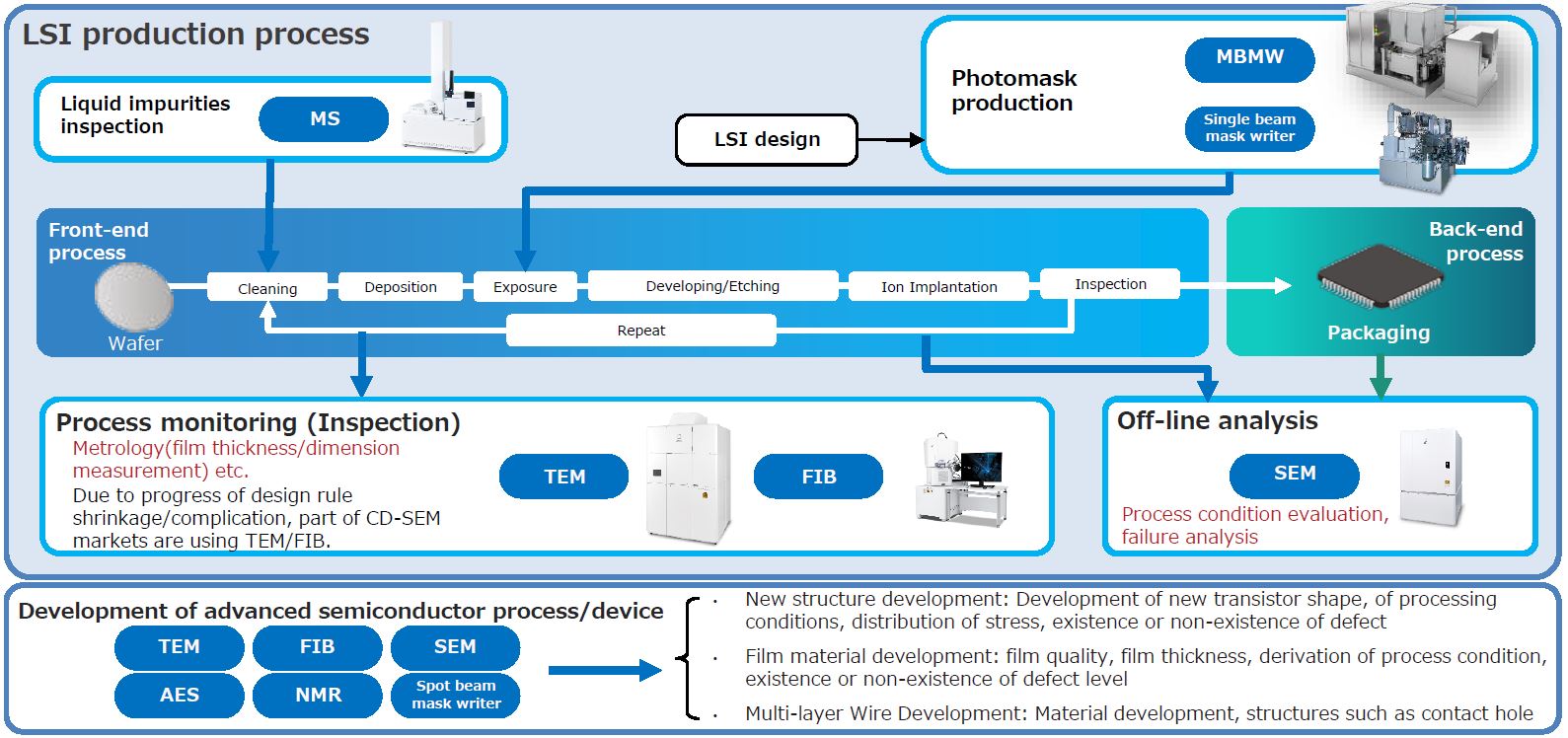
2. JEOL Semiconductor-Related Products and Their Applications
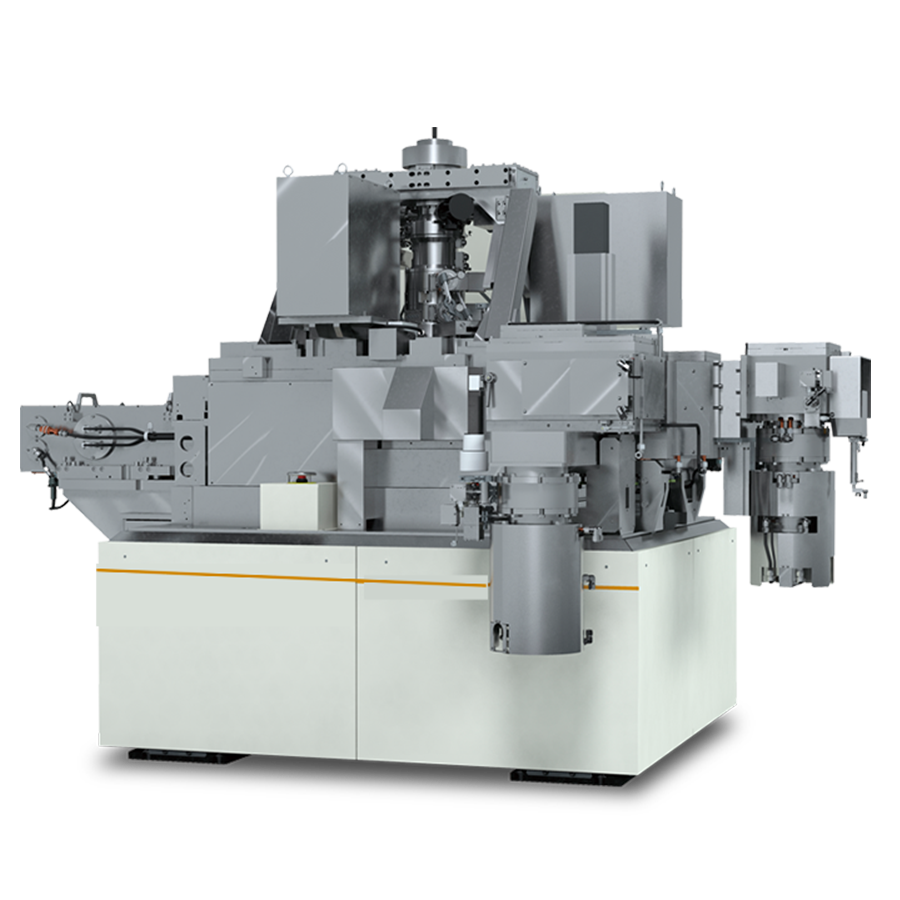
3. EB:Electron Beam Lithography System
EB lithography system is used to draw IC and circuit data designed with EDA(Electronic Design Automation)tools. The patterns are drawn onto glass or wafer substrates using EB lithography system.
JEOL's EB lithography systems are advanced technology, achieving high speed, high precision and high reliability. This EB system uses a variable-shaped 50 kV electron beam and a step-and-repeat stage.
4. FIB-SEM/TEM:Application of TEM-Based CD Measurement in Advanced Semiconductor Processes
TEM-LINKAGE
JEOL adopts a double tilt cartridge that facilitates integration with the TEM.
This cartridge is easily mounted onto a double-tilt TEM holder, eliminating any need to remove or exchange the FIB grid.
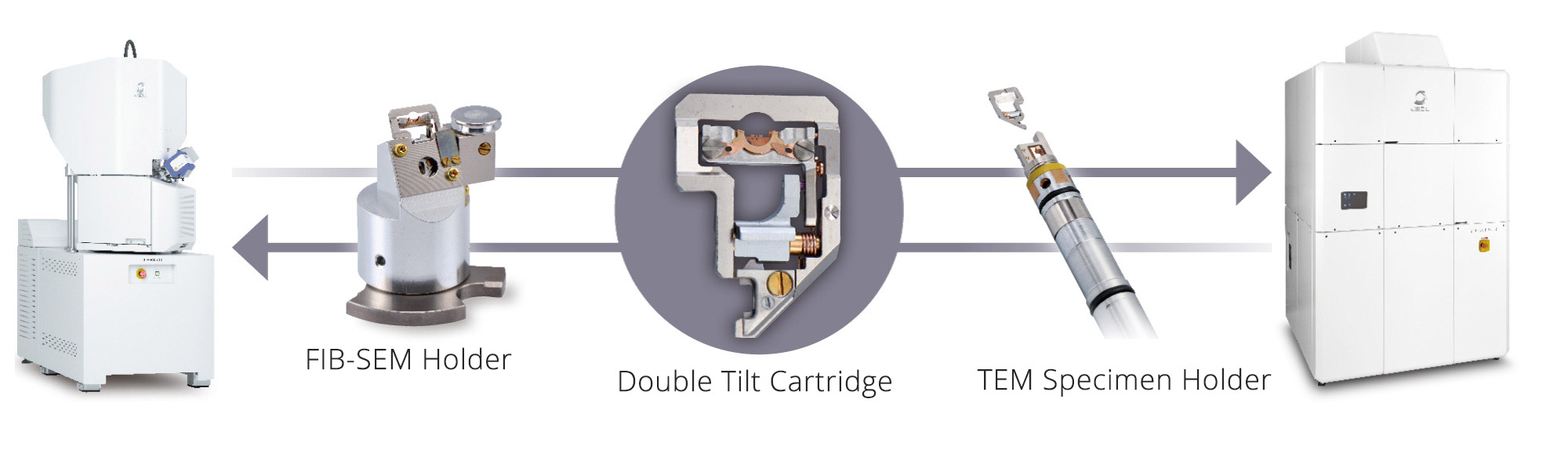
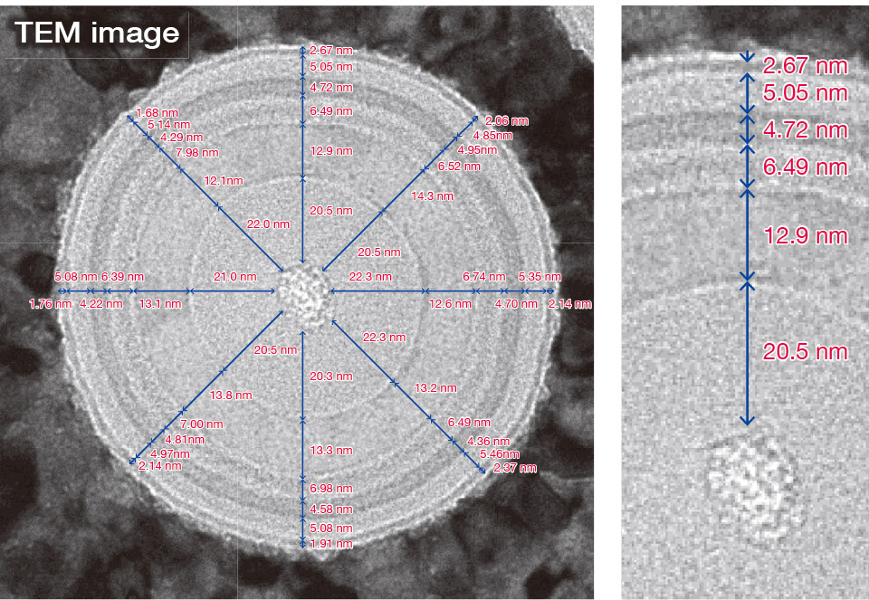
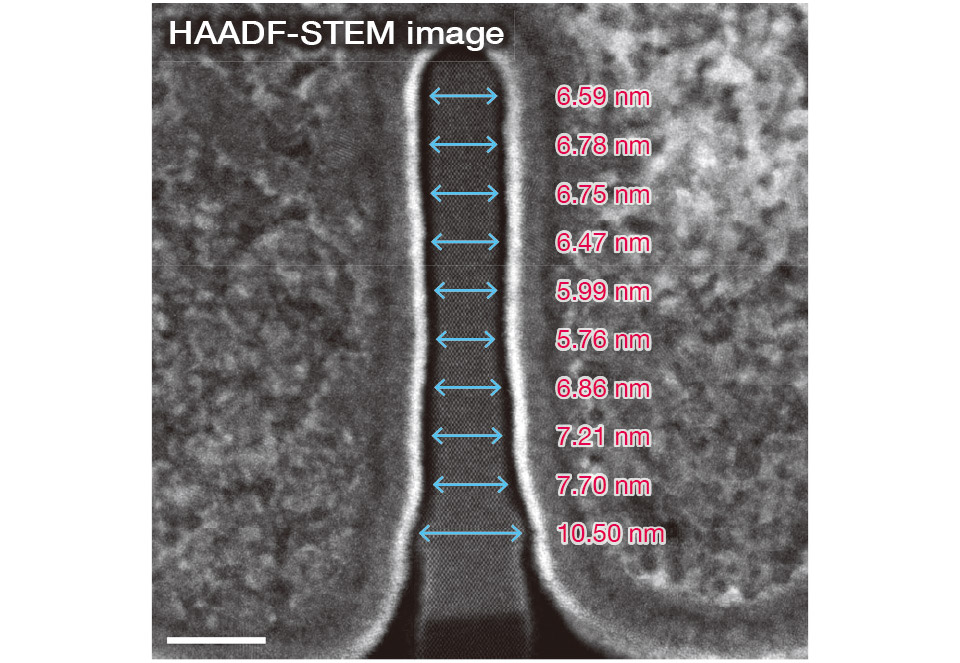
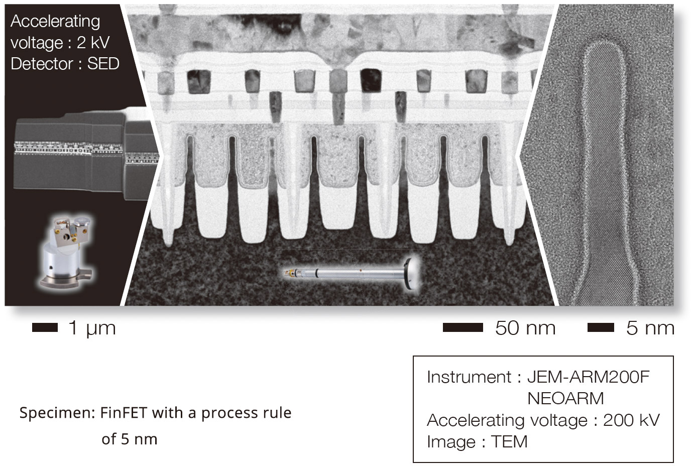
The figures below show a HAADF-STEM image of a Fin Field-Effect Transistor (FinFET) and a TEM image of a flash memory, both acquired using the JEM-ACE200F. Multi Image Tool developed by SYSTEM IN FRONTIER INC. is used for the measurement, enabling operators to create customized measurement recipes.
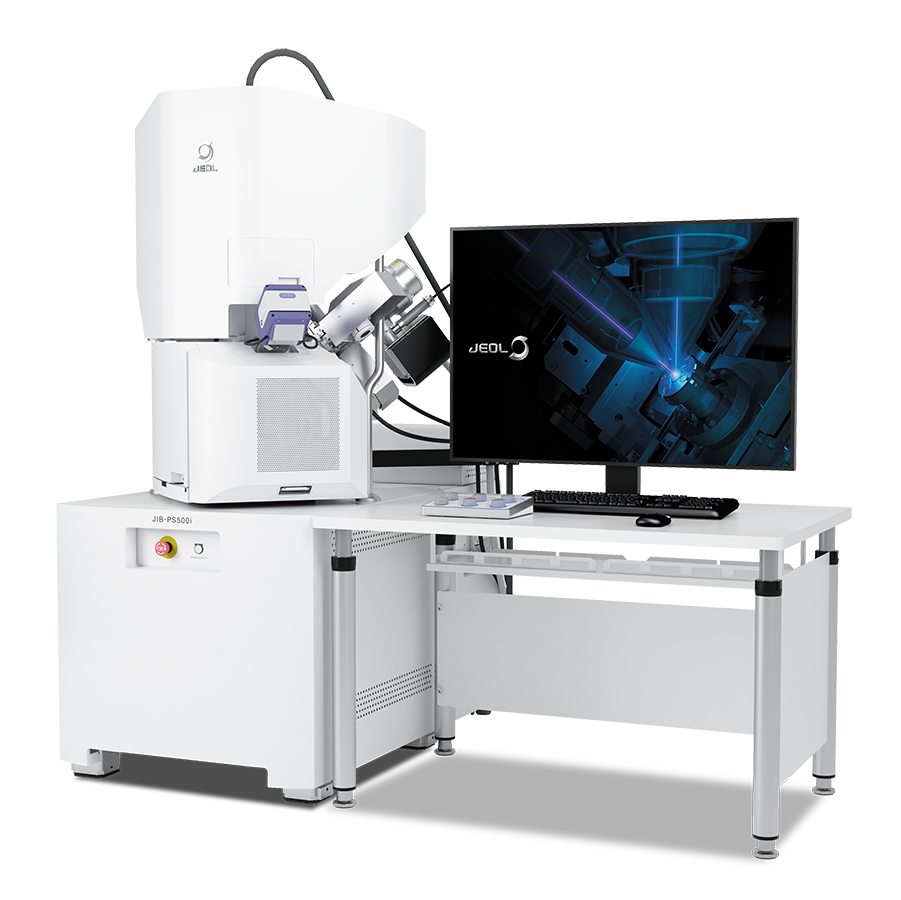
JIB-PS500i FIB-SEM system
The JIB-PS500i provides three solutions to assist TEM specimen preparation. High throughput workflow is assured from specimen prepartion to TEM observation.
JEM-ACE200F High Throughput Analytical Electron Microscope
The JEM-ACE200F is an electron microscope responding to the system allowing for an operator to obtain data without operating the electron microscope by creating recipes for operation workflow.
Since the JEM-ACE200F inherits hardware technologies of the JEM-ARM200F high-end TEM and the JEM-F200 multi-purpose FE-TEM, this new high throughput analytical electron microscope provides superbly high stability and analytical capabilities with a renewed sophisticated exterior design.
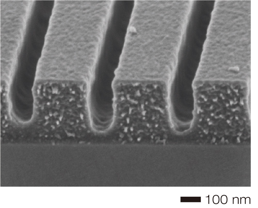
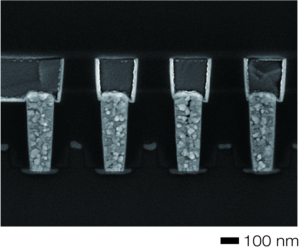
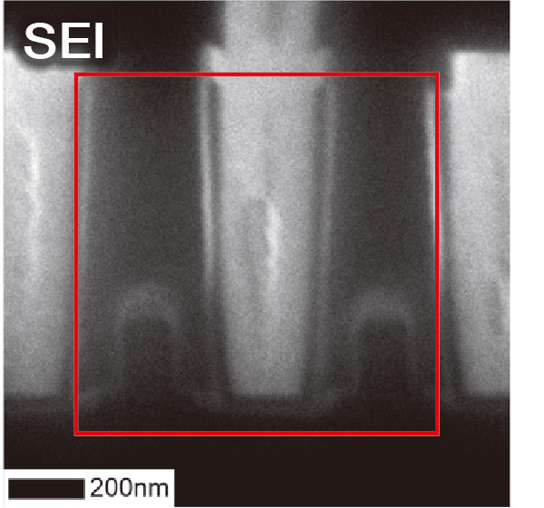
Creating a TEM Specimen of a FinFET
The figures on the left are an SE and BSE image of a FinFET. You can capture high-contrast images to target processing end points.
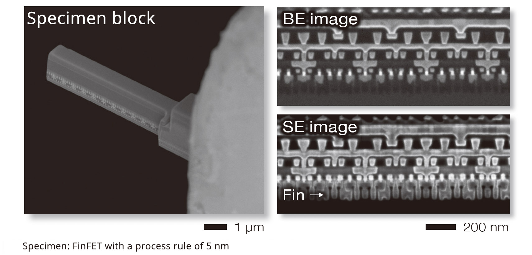
The FIB-SEM is capable of precisely thinning the Fin section region of interest. Using the DT transfer cartridge, you can move the specimen into a double tilting TEM holder for high resolution observation.
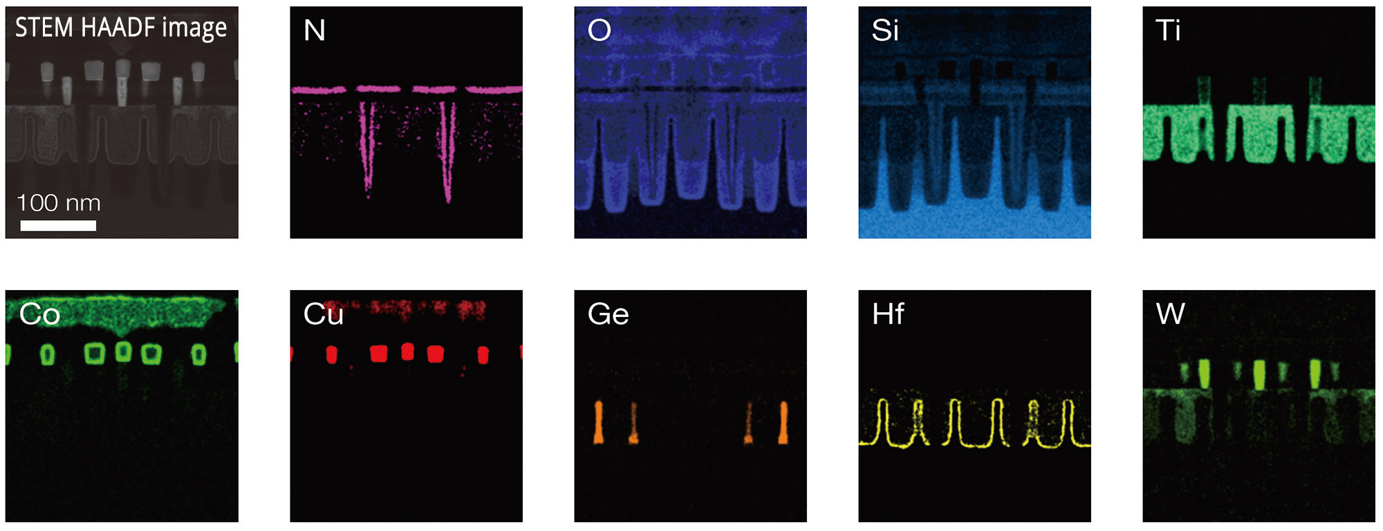
Structural and Compositional Analysis of FinFET
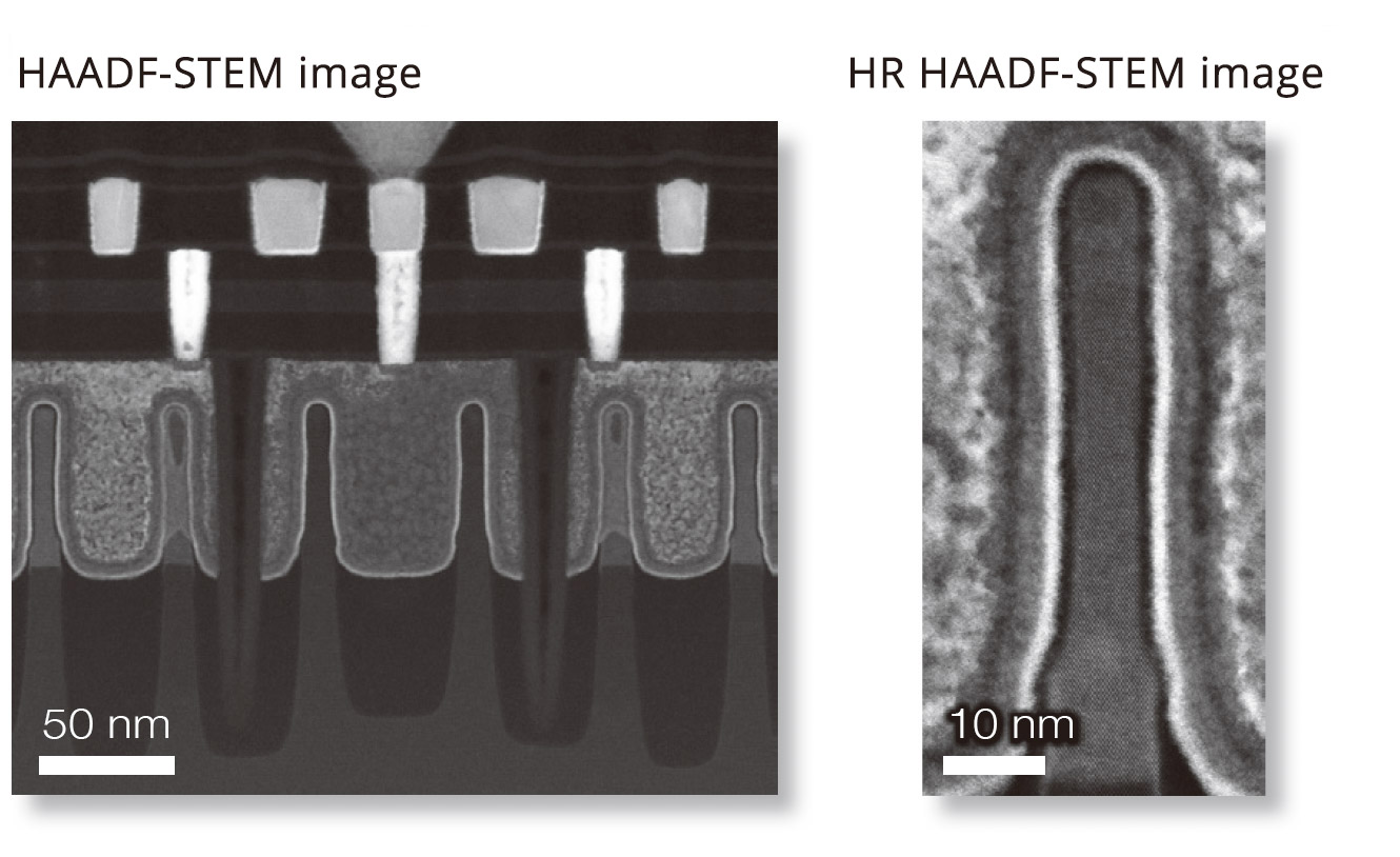
The figures on the left show an HAADF-STEM image and EDS maps of a FinFET. The shape of the FinFET, the structure around the gate, the arrangement of the contact region, and the elemental distribution can be clearly observed. In particular, the HAADF-STEM image provides a clear view of the gate insulating films (SiO2 and HfO2) as well as the layer structure of the metal gate.
Specimen: FinFET with a process rule of 5 nm
Accelerating voltage: 200 kV
EDS maps (net count maps)
5. SEM:SEM Functions for Observing and Analyzing Semiconductor Devices
A SEM is an instrument that scans the specimen surface with a fine electron beam to observe it. By leveraging attachments, such as EDS, CL, and Raman, various information, such as elemental analysis, crystal defects observation, and stress measurements, can be obtained.
The JSM-IT810 is equipped with Neo Engine, a next-generation electron optical control system, and SEM Center, which offers highly user-friendly operation, such as Zeromag and EDS integration. In addition, the automatic observation and analysis function Neo Action and the automatic calibration function not only improve efficiency and productivity, but also contribute to the elimination of labor shortages.
Resist
SRAM
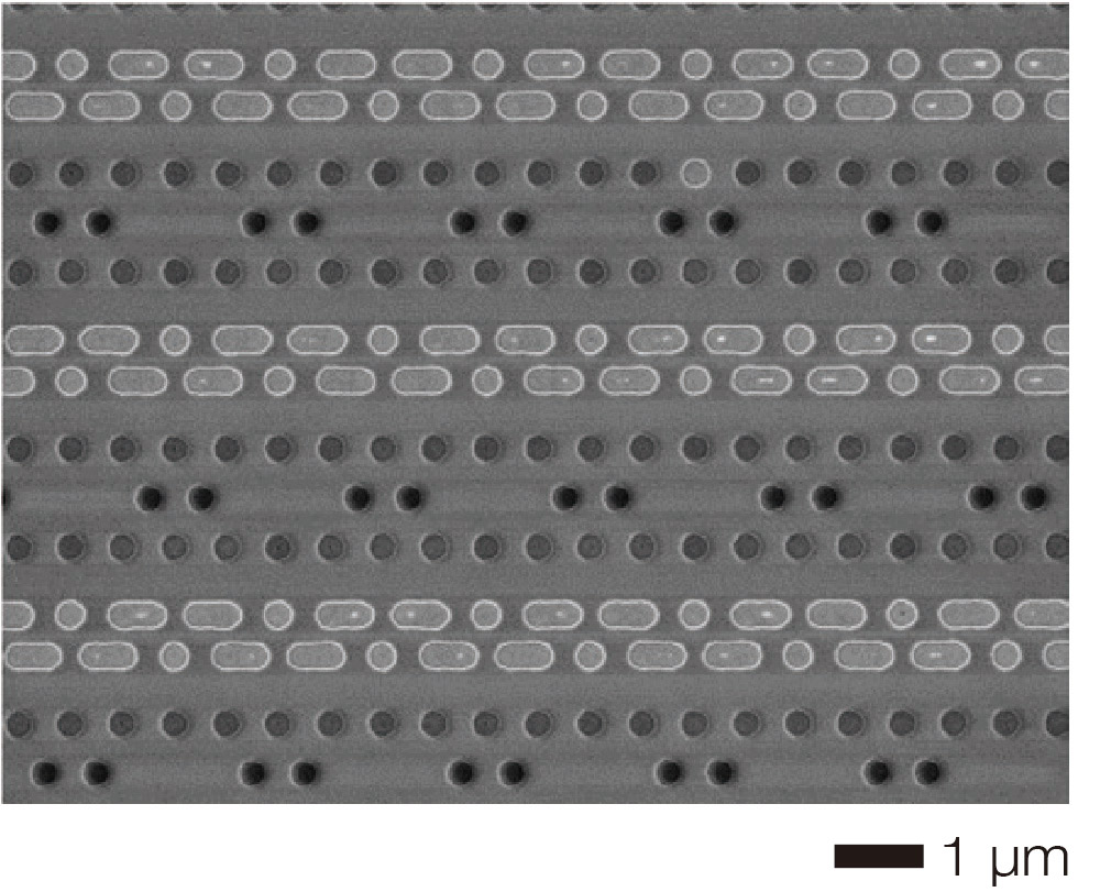
IC cross section
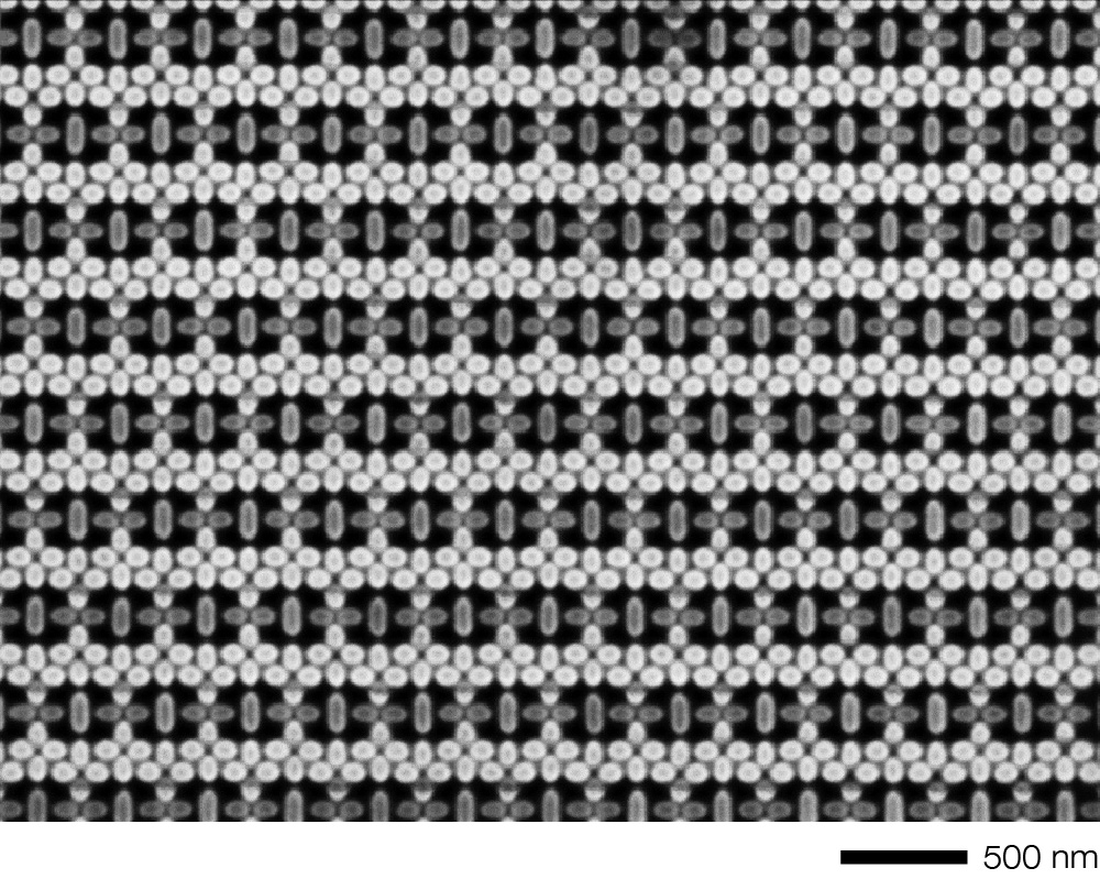
Voltage Contrast Observation of the Semiconductor Multi-Chip After SRAM delayering
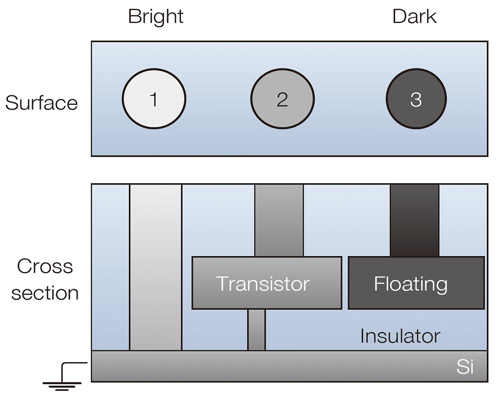
Schematic diagram of the voltage contrast (VC)

Surface Observation Specimen Holder -
SM-71230SOHD
The voltage contrast (VC) is a contrast that occurs in the SEM image by the difference in the conductivity on the surface of the semiconductor device. For example, if a defect occurs in a tungsten plug, the defective plug shows a different contrast compared to the normal plug. This can be used to locate the defect.
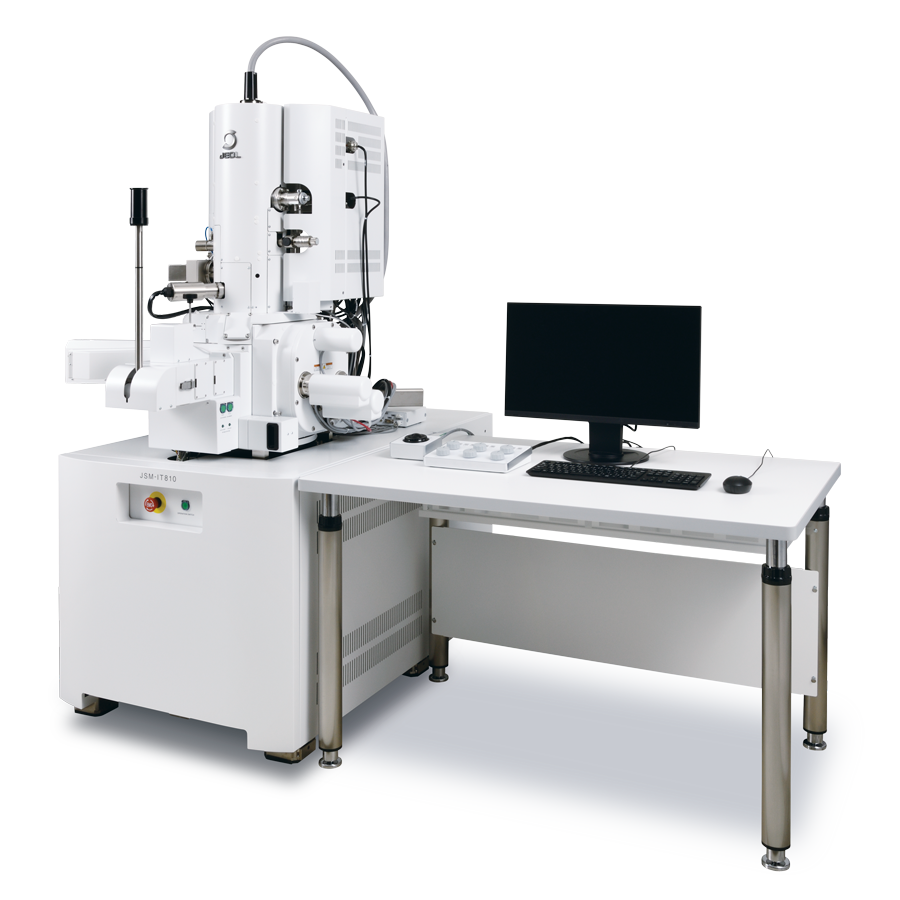
JSM-IT810 Schottky Field Emission Scanning Electron Microscope
Versatility and high spatial resolution meet automation with the JSM-IT810 series FE-SEM.
No-coding automation for imaging and EDS analysis is built-in for a streamlined and efficient workflow.
New functions are available to ensure high quality data and an enhanced user experience for all SEM users.
Functions include the SEM automatic adjustment package, a trapezoidal correction function (useful for EBSD measurements) and Live 3D surface reconstruction for observation of surface topography.
Operating a FE SEM has never been easier with the JSM-IT810 series.
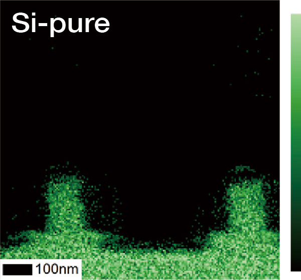
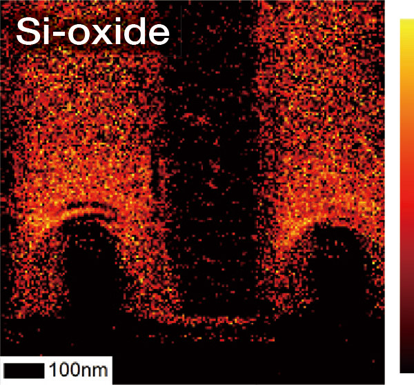
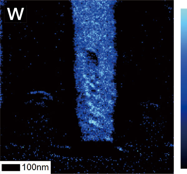
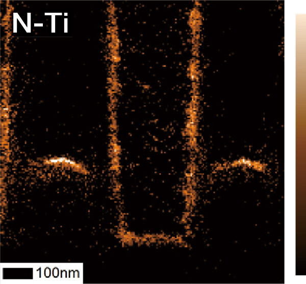
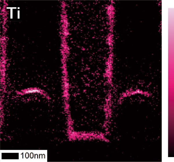
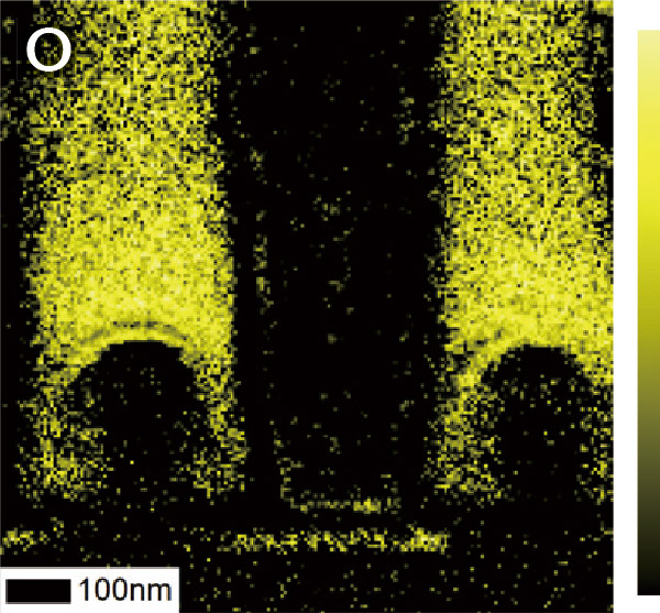
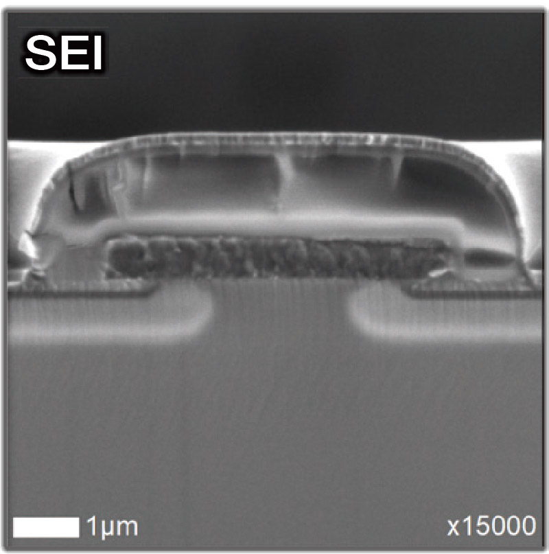
6. AES/CP:Visualization of Elements and Distribution by Chemical State in Semiconductor Multi-Chip CP Cross Sections
Cross-sectional analysis is often used in device failure analysis. However, high spatial resolution analysis is needed when analyzing miniaturized and complex devices.
AES allows for high spatial and energy resolution analysis of bulk specimens, making performing more detailed failure analysis simpler. As an example, a visualization of the distribution of the elements Si and SiO2 in different chemical states in the SRAM and CMOS region is given below.
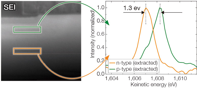
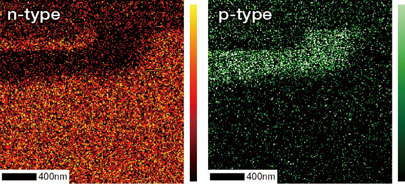
Internal Potential Diff erence Analysis on the pn junction in the Sic Power Semiconductor Diode
The pn junction forms the structure of the board in SiC Power Semiconductor Diodes and holds a vital role in the operation of the device. The performance of this bond is largely dependent on the amount of impurities and the doping process used for this as well as the process in the film formation.
Observation can be performed easily with voltage contrast (VC), but there are only limited techniques for detailed analysis of slight differences in dopant concentration with nanometer-order resolution.
Using AES, the internal potential difference can be evaluated from the amount of shift in the kinetic energy peak. Here, the SiC power semiconductor pn junction was analyzed. The position of the Si KLL peaks in the p-type region and n-type region differ by 1.3 eV. This energy difference was used to visualize the p-type and n-type regions.
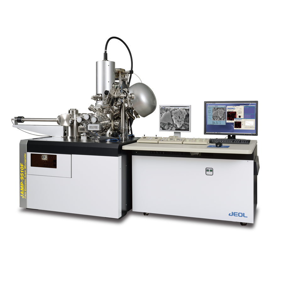
JAMP-9510F Field Emission Auger Microprobe
It is a high specification Auger electron spectrometer with a hemispherical analyzer to provide high throughput analysis of the chemical bonding state at nano to micro areas, and a field emission electron gun also used for EPMA, because it can deliver a large, stable electric current The highly precise eucentric specimen stage makes it possible to perform the previously-impossible analysis of insulators.
This in combination with the floating type ion gun offers the versatility to handle any specimen, such as metals and insulation materials, to obtain composition information to and chemical information.
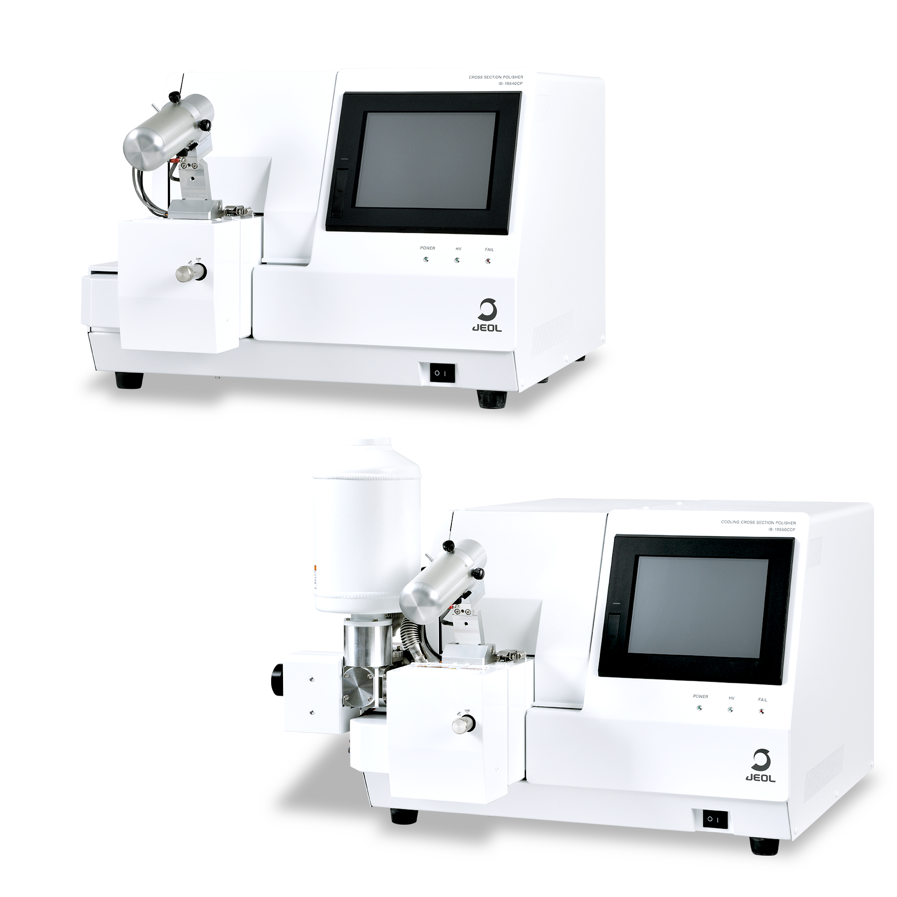
IB-19540CP CROSS SECTION POLISHERTM / IB-19550CCP COOLING CROSS SECTION POLISHERTM
CROSS SECTION POLISHERTM (CP) is a device to prepare a cross section of a specimen for electron microscopy.
Since a cross section is prepared with an ion beam, it is possible to obtain a good quality cross section in a shorter time without individual differences, compared to other methods such as polishing, which requires experience.
Incorporating the new GUI and Internet of Things (IoT), operation and monitoring of milling process became more user-friendly with the IB-19540CP/IB-19550CCP.
High throughput ion source and high throughput cooling system enable rapid and smooth cross section preparation.
Semiconductor Note
JEOL instruments and their applications for Semiconductor are listed in PDF. Please take a look at this PDF as well.
To view applications on Semiconductor more, click button below.