3D NAND TEM Specimen Preparation by FIB-SEM
IB2025-03
Introduction
FIB-SEM is a system integrating fine processing by using a Ga ion beam and observation & analysis function by SEM. This feature enables precise preparation of TEM specimens while checking cross-sectional images during processing. In particular, in the field of semiconductors where miniaturization continues, it is widely used for a TEM specimen preparation from the desired location. 3D NAND is a NAND type flash memory and is widely adopted in the storage device of a smartphone and PC. It consists of regularly stacked fine structures ranging from tens to hundreds of nanometers (Figure 1). TEM analysis is generally performed for quality testing. Therefore, the FIB-SEM is indispensable for high-precision specimen preparation prior to TEM observation.
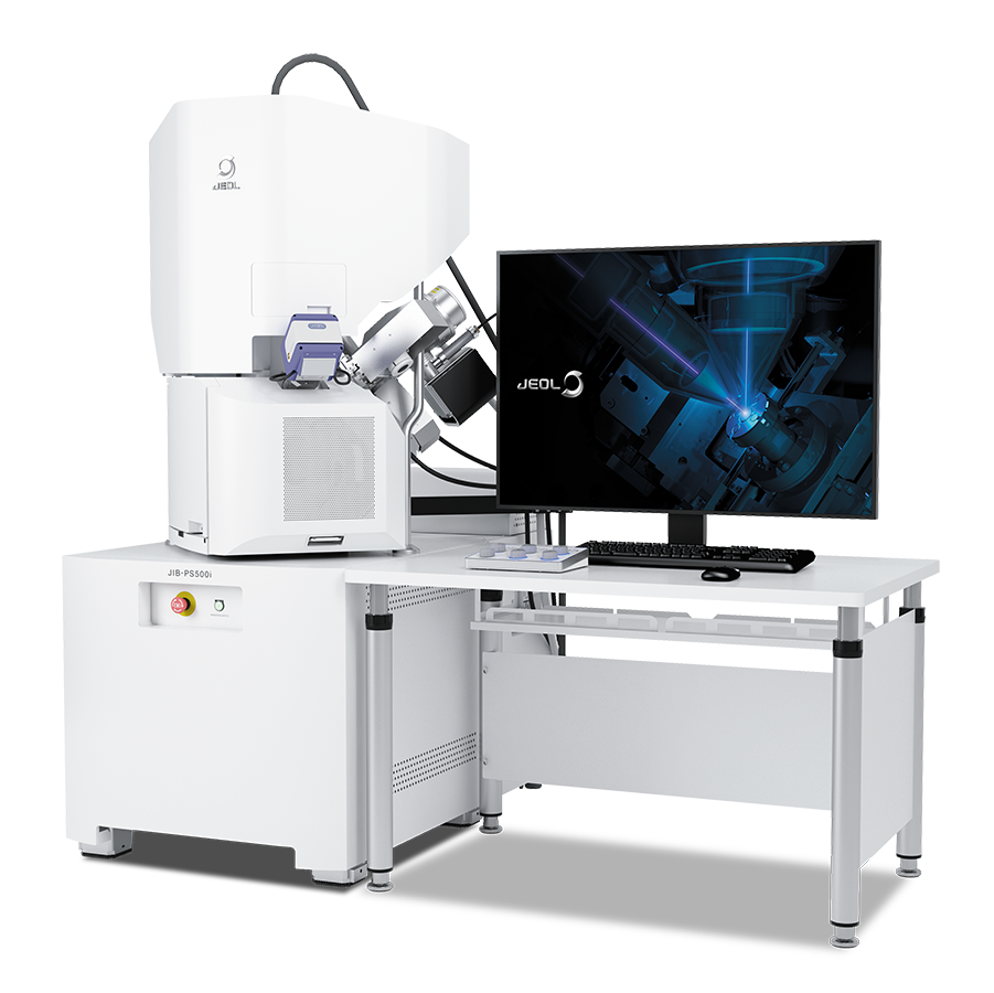
In this application note, we used the FIB-SEM system "JIB-PS500i" (Figure 2), which incorporates a high-resolution SEM and supports a streamlined STEM workflow, to obtain SEM images and prepare TEM specimens from three directions of the 3D NAND structure. The TEM observation results obtained are presented.
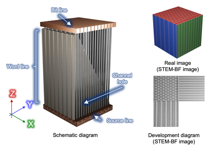
Figure. 1 3D NAND Structure
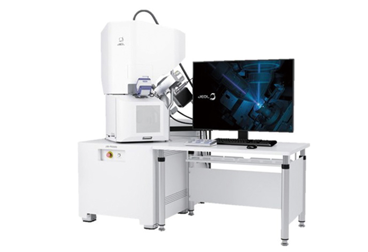
Figure. 2 JIB-PS500i Appearance
Steps of TEM specimen preparation by FIB
In TEM specimen preparation using the FIB for 3D NAND, the conventional method involves cutting a block from the substrate material, mounting it onto the FIB grid, and then thinning the block. With JIB-PS500i, since the stage can be tilted by more than 90 °, confirmation of TEM specimens using STEM is possible without removing them from the system (Figure 3). This function allows for preparing a high-quality TEM specimen targeting a specific location.
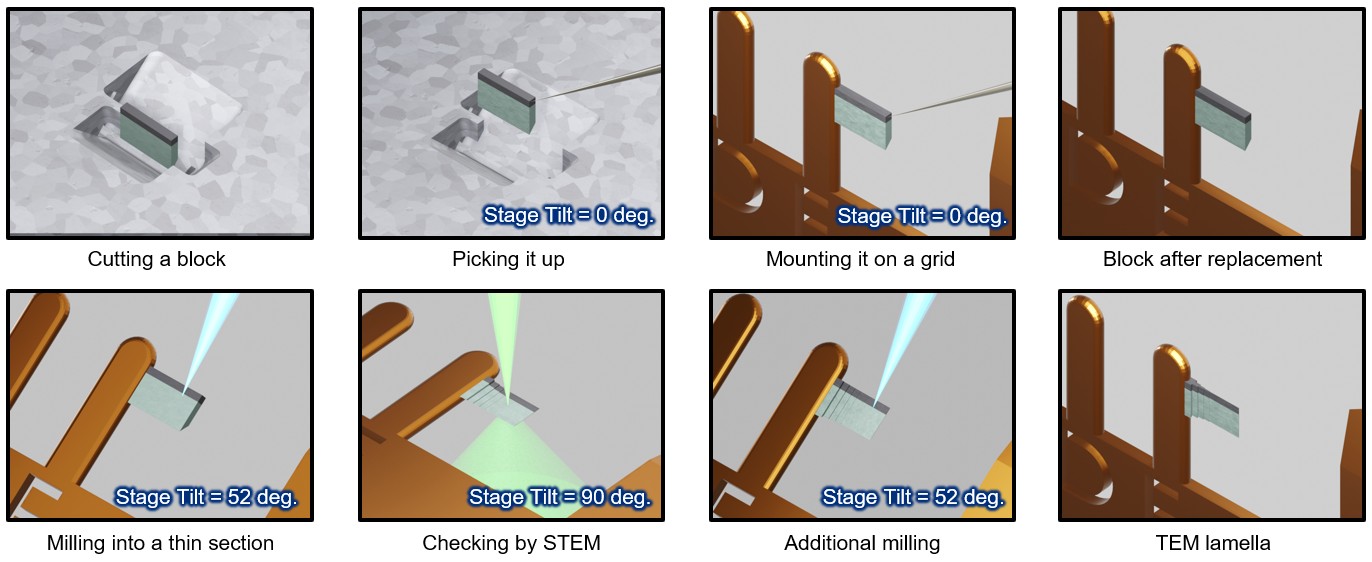
Figure. 3 Flow of TEM specimen preparation by using JIB-PS500i
Results
SEM images and SEM-STEM images (taken by JIB-PS500i), and TEM-STEM images (taken by JEM-ARM200F) from three directions (Figure 4 to 6) are shown below.
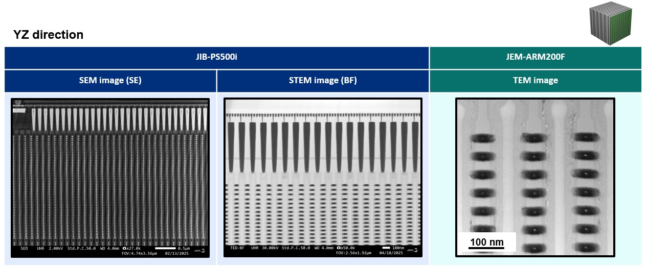
Figure. 4 SEM image, STEM image (JIB-PS500i) and TEM image (JEM-ARM200F) taken from YZ direction
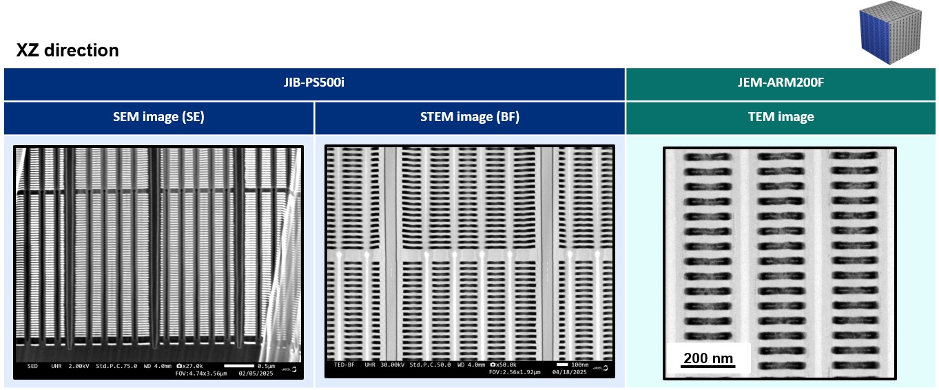
Figure. 5 SEM image, STEM image (JIB-PS500i) and TEM image (JEM-ARM200F) from XZ direction
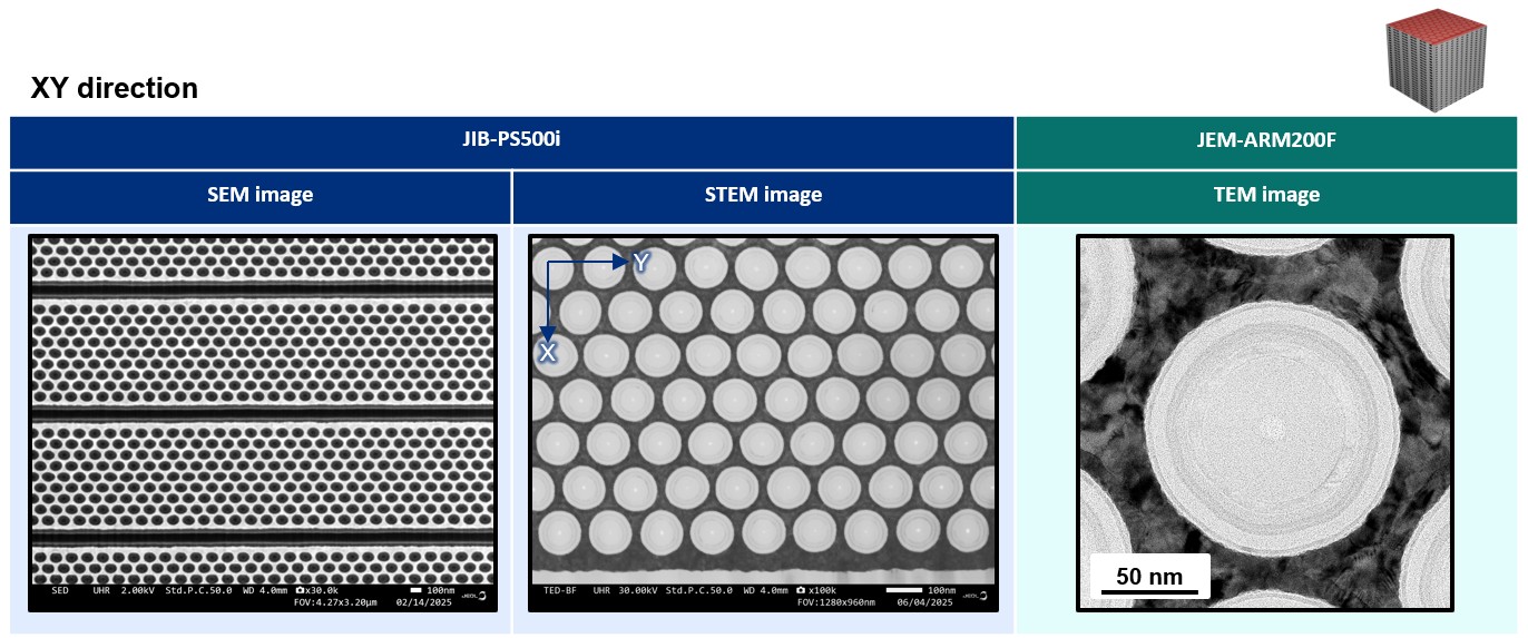
Figure. 6 SEM image, STEM image (JIB-PS500i) and TEM image (JEM-ARM200F) from XY direction
Conclusion
Using the JIB-PS500i, SEM observation and TEM specimen preparation for 3D NAND were performed from three directions.
High-quality TEM specimens can be prepared even for fine semiconductor structures such as 3D NAND, due to the high-resolution SEM image and easy STEM observation.
Solutions by field
Electrical / Electronic Component
Related products
Are you a medical professional or personnel engaged in medical care?
No
Please be reminded that these pages are not intended to provide the general public with information about the products.