Diamond Semiconductors, Practical Application Just Around the Corner
INTERVIEW 14
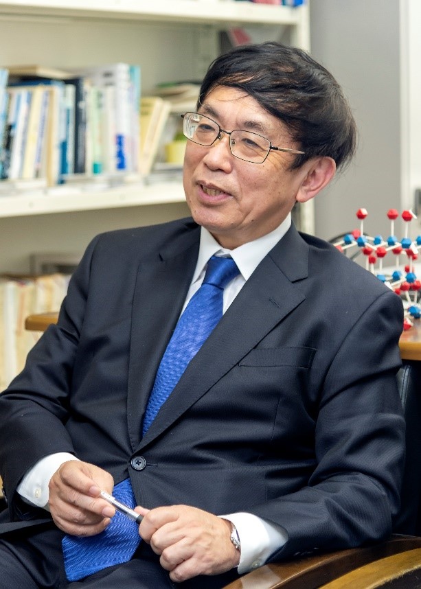
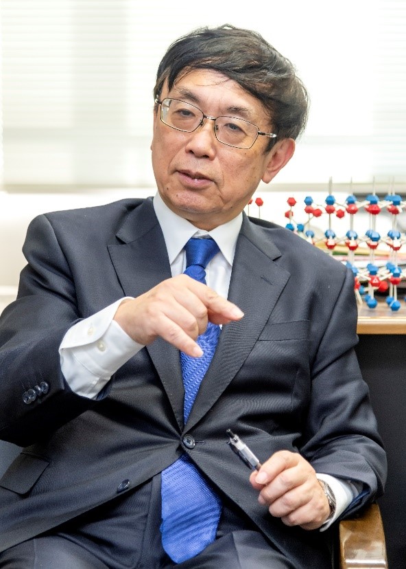
Prof. Makoto Kasu
Department of Electrical and Electronic
Engineering
Saga University
Diamond semiconductors have been attracting attention as power semiconductors and high-frequency devices. Recently, movements have been seen, demonstrating that it had stepped away from the basic research to a practical application. Prof. Makoto Kasu, Saga University has been engaged in research about the practical applications of diamond semiconductors. We interviewed him about his stories on research and the project for practical application.
Semiconductors corresponding to EV and "Beyond 5G"
Prof. Kasu's research on diamond semiconductors began involving people around him.
He first announced that he would begin developing a microwave electricity amplifying device for space communication, with Japan Aerospace Exploration Agency (JAXA) and the National Institute of Technology (KOSEN), Kure College (December 2023). The aim was to install the device in an ultra-small satellite for further demonstration in space. One year after the announcement, he began collaborating with CTC (ITOCHU Techno-Solutions Corporation) about research towards the social implementation of diamond semiconductors (January 2025). In addition, Prof. Kasu plans to establish a new company called "Diamond Semiconductor" to accelerate the movement. Within the fiscal year 2026, he plans to ship diamond semiconductor samples from this new company.
Diamond semiconductors are gaining attention because they offer various potentials that far exceed those of silicon (Si), and they are expected to be used in the fields where silicon is not suitable.
For example, the demand for power semiconductors which controls electricity, such as electric vehicles
(EV) are increasing. However, the required features are a high dielectric breakdown strength and the
ability to easily conduct the current in areas where carriers (free electrons or holes) are present.
The dielectric breakdown strength of diamond semiconductors is 33 times that of silicon one and allowing
for large electric currents where carriers are present. In the index to indicate power semiconductor
performance (Baliga's figure-of-merit), the diamond semiconductors have a higher value than silicon, as
well as the next generation power semiconductors of silicon carbide (SiC) and gallium nitride (GaN).
| Si | SiC | GaN | Diamond | Feature of diamond semiconductor | |
|---|---|---|---|---|---|
| Band gap | 1 | 2.9 | 3.0 | 4.9 | Operates at temperature 5 times higher |
| Dielectric breakdown strength | 1 | 9.3 | 16.6 | 33 | Operates at a voltage 33 times higher |
| Thermal conductivity | 1 | 3.8 | 1.2 | 17 | 17 times easier to dissipate heat. No temperature rise. |
| Baliga's figure-of-merit: (BFOM) | 1 | 580 | 3,800 | 49,000 | Device characteristics of high efficiency with 50,000 times higher electric power |
| Johnson's figure-of-merit: (JFOM) | 1 | 420 | 1,100 | 1,225 | High speed power device characteristics for 6G with 1,200 times power. |
Physical property of diamond semiconductor (Material provided by:Prof. Kasu)
In addition, the index indicating the suitability of a high frequency device (Johnson's figure-of-merit) is also high. Therefore, its use is expected at the mobile phone base of "Beyond 5G (*1). Moreover, the diamond semiconductors are resistant to radiation and its use for communication in a space environment is highly expected.
As the research of diamond semiconductors began blooming in early 1980's, it is a
relatively new field. The trigger was the success of epitaxial growth (*2) of diamond film in Japan.
It was realized by MPCVD (Microwave Plasma Chemical Vapor Deposition), which is a reaction of raw material
gases of methane and hydrogen in plasma. Artificial diamonds used to be produced by applying high voltage
(approx. 50,000 atmospheric pressure) as if simulating the growth of natural diamonds in general. However, it
can now be produced with low pressure (for example, 0.1 atmospheric pressure). National Institute for Research in Inorganic Materials(then) (current: NIMS: National Institute for Materials Science) had found this method and
announced. Many researchers in Japan and outside of Japan began studying diamonds.
*1 Next generation (6G) information communication infrastructure that further enhances the performance of the 5th generation mobile communication system. Practical use is expected to begin around 2030.
*2 A technology for growing new single-crystal thin films on single-crystal substrates. When the substrate crystal and the crystal to be grown have the same lattice constant, it is called homoepitaxial growth, and when they have different lattice constants, it is called heteroepitaxial growth. In diamond semiconductors, heteroepitaxial growth is almost always used.
Device that flows electricity only in the morning and evening
Prof. Kasu started the research about diamond semiconductors at NTT Basic Research Laboratories came up with a question. When diamond thin films grown by MPCVD (*3) are left in the air, they sometimes conduct electricity. But the reason for this was not clearly understood. There were several theories. One theory that "it is caused by water and carbon dioxide (in the air)" was even published in a well-known overseas scientific journal. However, when Prof. Kasu immersed the film in water or blew on it, it did not conduct electricity as expected. What could be the cause?
"I should check it by myself". With that in mind, Prof. Kasu tried various gases found in the air such as nitrogen(N2), oxygen(O2), carbon oxide (CO2), and argon (Ar). But none of them conducted electricity.
One day, he noticed something strange in the measurement value. He applied voltage to the diamond for an electrical connection check and left it as is for over a week. Then, he found that a large electric current was flowing around 9 am and 5 pm. It was always 9 am and 5 pm on weekdays. On Saturdays and Sundays, the electricity did not flow. What on earth was going on?
3PM. It is time for tea, set aside by the research laboratory. Researchers from other departments gathered one by one, bringing tea and coffee with them. He brought up the topic of the "9 to 5 phenomenon." He wondered what everyone would say. "Could it be nitrogen dioxide (NO2)?" A woman from the chemistry department suggested.
NO2 is a gas contained in the exhaust gas of automobiles. So, its concentration increases during commuting hours. It was pointed out that this change is similar to the change in the current of the diamond. If commuting automobiles are the cause, it would also be consistent with the fact that there is no current on Saturdays and Sundays. He immediately borrowed a device to generateNO2 and a device to measure it and conducted an experiment. Sure enough, a current flowed.
Following that, he investigated whether other gases could produce the same effect and found that ozone (O3), sulfide oxide (SO2), and nitrogen monoxide (NO)(*4) also conducted electricity. It is considered that these gases adhere to the surface, causing electrons to move from the hydrogen terminals to the gas molecules, and generating carriers on the diamond surface. He also conducted another experiment to see how carrier density changes when the type and concentration of gas is altered.
*3 Precisely, it is a diamond thin film with hydrogen bonded on the surface by being kept in hydrogen plasma atmosphere for about 30minutes even if methane is exhausted. It is called hydrogen terminated diamond.
*4 Gases other than O3 are the ones included in the exhaust gas of automobiles. O3 is generated by the photochemical reaction of NOx and HC in the exhaust gas by receiving ultraviolet from sun light. In other words, each of the 4 types of gases was attributed to the exhaust gas of automobiles.
As mentioned before, it is necessary that there are carriers existing in the semiconductor device to work. Currently, the basic method to generate carriers in the diamond semiconductor is a termination process (process to make other atoms such as hydrogen bonded on the surface of diamond film). In particular, the terminal process using hydrogen is said to be the most feasible method for practical application. This is a carrier generation method that is unique with diamonds, which is not performed with other semiconductors.
"What was the reason for conducting electricity when exposed to the air?". By facing the question Prof. Kasu had when he started the research, he could elucidate the type of inorganic molecules that can effectively induce carriers and data such as the concentration. These findings tuned out to become advantageous know-how for practical applications.
World's Highest Record in Electricity and Voltage
Research results for practical applications remarkably began increasing from about 2021. First, he invented Field Effect Transistor (FET) of new structure. By making a mechanism to the one that hardly deteriorated provides a longer lifetime of the device. This also achieved the highest level output power of 179MW/cm2 (as of April 2021). Six months later, these records have been renewed. The wafer diameter became 2 inches, with the increased output power to 345MW/cm2. (as of September 2021).
In the next year, the diamond semiconductor achieved the output power of 875MW/cm2, output voltage of 2586V (as of May 2022). These values are the world's highest records for diamonds (*5). Prof. Kasu's paper was posted in the "Electron Device Letters" journal of IEE (Institute of Electrical and Electronics Engineers) with covering the top page as the paper of the recent topic. In addition, with this outcome being evaluated, the diamond semiconductor was selected for an excellence award in semiconductor devices of the "Semiconductor of the year 2023" ("Electronic Device Industry News" of Sangyo Times Inc.).
In 2023, he conducted an operation verification of a power circuit with a diamond semiconductor built in. The switching movement was as fast as less than 10 ns, demonstrating that there is no problem in dynamic characteristics (April 2023). Continuous operations were also tested. There was no characteristic deterioration even after 190 hours of continuous operation. These efforts towards practical application in sight may have led to the movement to involve people around him, as mentioned at the beginning of this interview.
*5 This record still remains as the world's highest record currently as of April 2025.
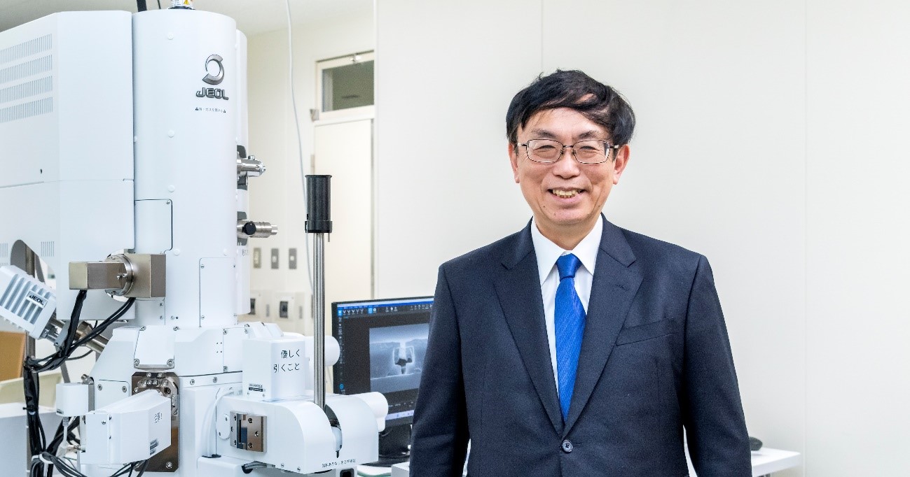
Introduction of electron beam lithography system and scanning electron microscope, towards development of integrated circuit
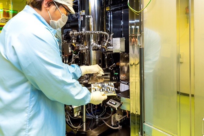
In April 2024, Prof. Kasu introduced an expensive instrument - an electron beam lithography system. Naturally, this is for developing an integrated circuit (IC). His diamond research came to the stage to develop an IC. To be concrete, the development of a microwave electricity amplifying device for space communication is assumed, as mentioned at the beginning.
The electron beam lithography system that he purchased was "JBX-8100FS" of JEOL Ltd. He was also offered a lower cost product by another manufacturer. But Prof. Kasu thought that "to purchase an instrument is to purchase its technology", and he declined that offer. The electron beam lithography system will be used by researchers who are not familiar with its operation. Speedy development is not possible without a product with easy-to-understand operation, reliability, and good technical support. JAXA (Japan Aerospace Exploration Agency), his research partner also readily agreed to allot most of the budget to the electron beam lithography system.
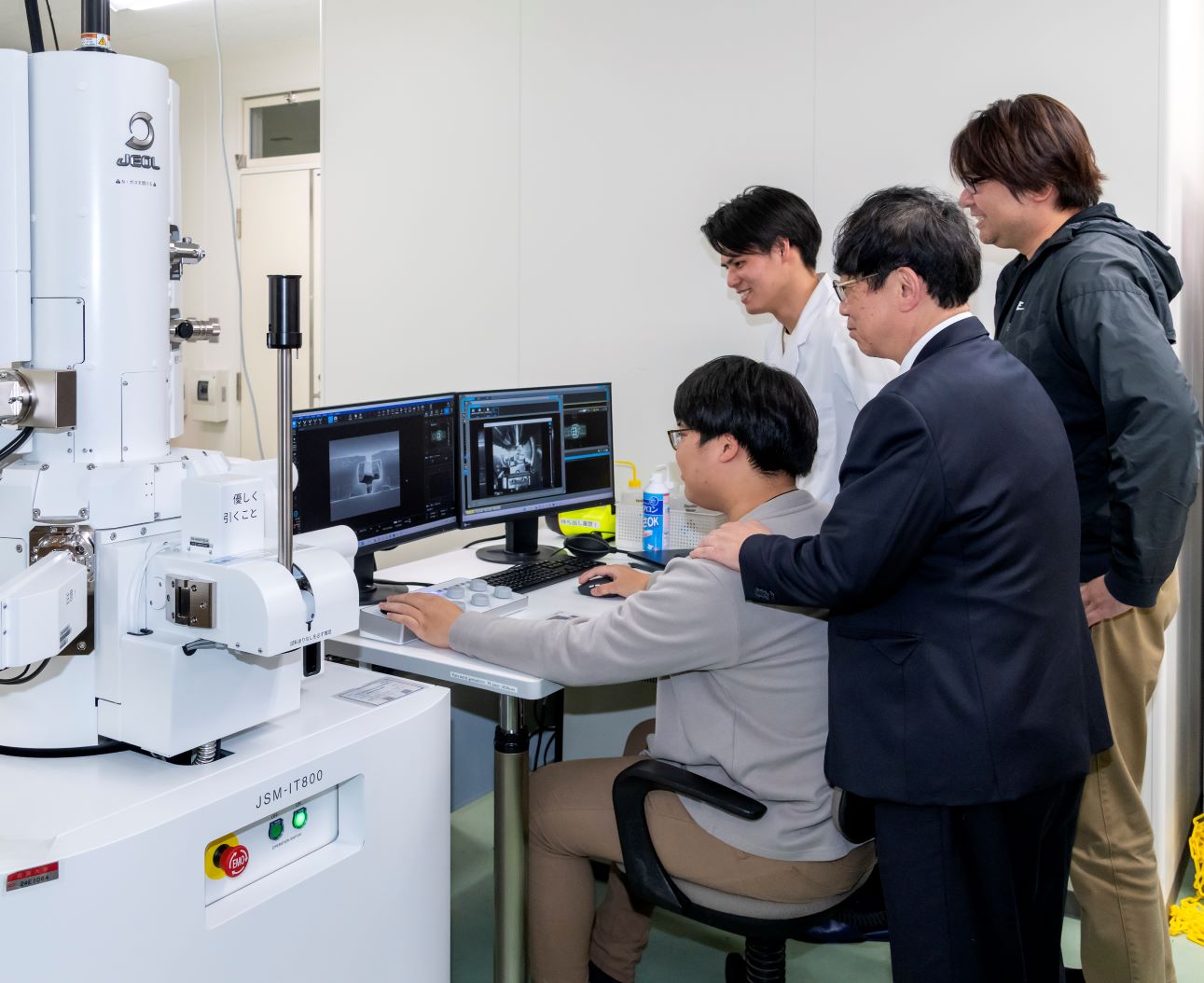
In September of the same year, he also introduced another instrument of JEOL. The Schottky field emission scanning electron microscope "JSM-IT800 (i)". This would be used to confirm the inside of a semiconductor device such as its compositions.
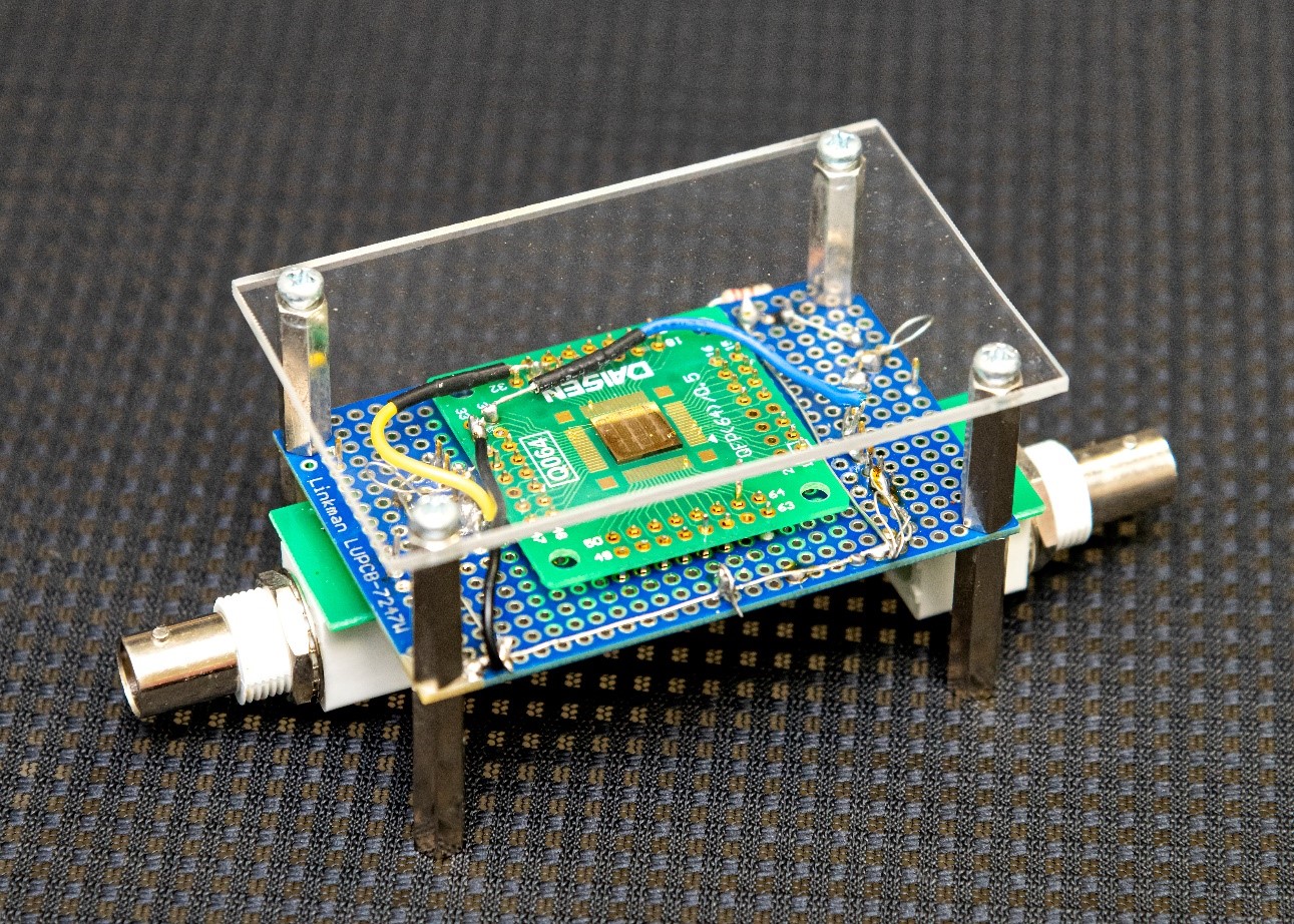
The transistor for a microwave produced by using the JBX-8100FS was announced at the 2025 JASP (Japan Society of Applied Physics) Spring Meeting (Friday, March 14, 2025, to Monday, March 17, 2025, at Noda campus, Tokyo University of Science). The image posted is the one taken by using the JSM-IT800 (i).
Actually, it is not only Saga University that has promoted the practical application of diamond semiconductor. Several venture companies are raising their hands, in Japan alone. Therefore, "we would like to implement the research with sense of speed" (Prof. Kasu). Prof. Kasu is hoping to promote this project with a sense of mission so that the diamond semiconductor can be developed as an industry born in Saga, Japan.
The development of microwave power amplification devices for space communications, which is being jointly promoted with JAXA and Kure College, is probably the one that is attracting the most attention from society. This project is for 5 years from fiscal 2023. By the end of fiscal 2028, when the project will be completed, the device is scheduled to be completed. The outcome will be reported by newspapers, etc. Until that time, JEOL instruments and technology will continue its contribution.
Makoto Kasu
Department of Electrical and Electronic Engineering, Saga University
1990 Joined Nippon Telegraph and Telephone Corporation and belonged to the basic research laboratories. While being engaged in research activities, he also played the role of lecturer and researcher at universities in Japan, Germany, and France, JAXA, Institute of Space and Astronautical Science.
2011 Professor of Graduate School, Saga University.
( https://www.sao.saga-u.ac.jp/admission_center/ouensite/research/01/ )
Posted: June 2025
Product Information
JBX-8100FS Series Electron Beam Lithography System
JSM-IT800 Schottky Field Emission Scanning Electron Microscope