JBX-8100FS Series
Electron Beam Lithography System
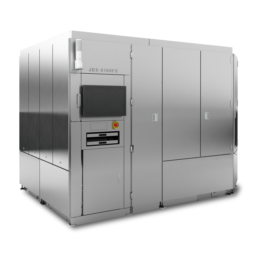
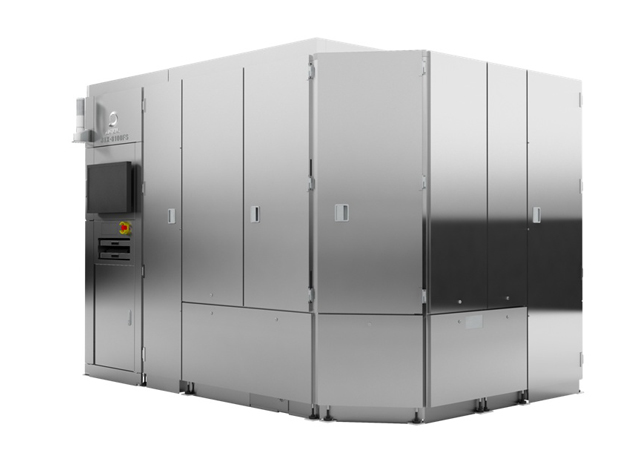
Spot type Electron Beam Lithography System JBX-8100FS achieved high throughput, small footprint and electric power saving.
Features
Small footprint
The area required for the standard system is 4.9 m (W) x 3.7 m (D) x 2.6 m (H), much smaller than the conventional systems.
Low power consumption
Power needed for normal operation is approximately 3 kVA, reduced to 1/3 of the conventional systems.
High throughput
The system has two exposure modes, high resolution and high throughput modes, supporting different types of patterning from ultra fine processing to small to mid size production. It has minimized the idle time during exposure while increasing the maximum scanning speed by 1.25 to 2.5 times to 125 MHz (the world’s highest level) for high speed writing.
Version
The JBX-8100FS is available in 2 versions: G1 (entry model) and G2 (full option model). Optional accessories can be added to the G1 model as needed.
New Functions
An optional optical microscope is available to enable examination of patterns on the sample without exposing resist to light. A signal tower is provided as standard for visual monitoring of system operation.
Laser positioning resolution
Stage positions are measured and controlled in 0.6 nm steps as standard, and in 0.15 nm steps with an optional upgrade.
System control
Versatile Linux® operating system combined with a new graphic user interface provides ease in operation. The data preparation program supports both Linux® and Windows®.
200 kV Model!
Maximum Accelerating Voltage To the world of 200 kV
JBX-8100FS is a Direct Writing EBL System with Gaussian Beam Optics designed to implement High Throughput and High Precision requirements from a wide range of applications.
The modular and upgradeable platform supports variety of fields from fabrication of advanced nanostructures to production of Compound Semiconductor Devices.
Enabling advanced applications such as holography, gray scale and micro-lens arrays
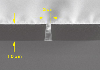
The images below are the EBL comparison between 100 kV and 200 kV.
200 kV demonstrates a reduced tapering effect with considerably thick resist.
Accelerating Voltage comparison between 100kV and 200kV (Sample: 10um thick resist)
Accelerating Voltage 100 kV
3,000 μC / cm2
Accelerating Voltage 200 kV
5,000 μC / cm2
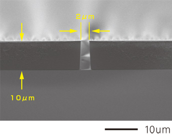
Resist : PMMA
Thickness : 10um
Field size : 500um
Pattern width : 2um
Substrate : Si
Notices:
Windows is a registered trademark of Microsoft Corporation in the United States and other countries.
Linux® is the registered trademark of Linus Torvalds in the U.S. and other countries.
Specifications
| Version | G1 (Entry model) | G2 (Full option model) | G3 (200kV model) |
|---|---|---|---|
| Writing method | Spot beam, vector scan, step and repeat. | ← | ← |
| Acceleration voltage | 100 kV | 100 kV / 50 kV | 200 kV / 130 kV / 100 kV / 50 kV |
| Beam current | 5 × 10-12 to 2 × 10⁻⁷ A | ← | ← |
| Field size | Maximum 1,000 μm × 1,000 μm | Maximum 2,000 μm × 2,000 μm | ← |
| Scanning speed | Maximum 125 MHz | ← | ← |
| Stage movable area | 190 mm × 170 mm | ← | ← |
| Overlay accuracy | ≦±9 nm | ← | ≦±8 nm |
| Stitching accuracy | ≦±9 nm | ← | ≦±8 nm |
| Electric requirements (Normal) | 3kVA | ← | ← |
| Substrate size | Maximum 200mmΦ wafer
6 inch mask blanks Small sample of any size |
← | ← |
| Substrate transfer | Single auto loader | 12 cassettes auto loader | ← |
| Major installable Options | Optical microscope
25 kV high voltage program Data preparation program additional license High resolution laser beam control system |
||
Catalogue Download
JBX-8100FS Series Electron Beam Lithography System
Application
Application JBX-8100FS
Development of the JBX-8100FS Electron Beam Lithography System
Gallery
More Info
Are you a medical professional or personnel engaged in medical care?
No
Please be reminded that these pages are not intended to provide the general public with information about the products.