Development of the JBX-8100FS Electron Beam Lithography System
JEOL NEWS Vol.53 No.10
Yukinori Aida
SE Business Unit, JEOL Ltd.
An Electron Beam Lithography system (hereafter EBL) is a product that can reproduce data designed by a user onto a silicon substrate or photomask blank. The shape of the electron beam will vary according to the application. A spot type electron beam (hereafter SB) is described in this report. The SB is an electron beam with a circular diameter of several nm, so it is possible to process patterns of less than 10 nm in size. With high-precision stage positioning technology incorporating a laser measurement system, it is possible to correct the position of the electron beam to compensate for errors in the stage stopping position. Conventionally, the application for SB with these features was mainly the research and development of next-generation semiconductor devices. Recently, however, the worldwide demand for SB has been growing as they are being used in production for a wide variety of communication devices and sensors. Applications can range from the production of sensors used for collision-prevention systems for automobiles to Distributed Feedback (DFB) lasers, which are used in the communication hubs for 4th generation communication systems (4G). To meet this demand, a new product, the JBX-8100FS, has been developed. This report introduces the JBX-8100FS series.
Introduction
The user creates pattern data using CAD, etc. This data can be replicated onto a substrate material by the EBL system, making it possible to perform nanofabrication. Since one of the goals in the manufacture of semiconductor devices is to make products smaller, the makers of the equipment used to manufacture semiconductors must develop equipment that can provide smaller pattern size. There is also a need to control the pitch with high accuracy of 0.1 nm or less for the production of DFB lasers, for example. This means that highly-accurate positioning is required. For research on nanoimprint template production, in addition to the accuracy described above, it is also necessary to achieve high positioning accuracy within the substrate. Furthermore, for the fabrication of transistors used in millimeter-wave devices, patterns must be overlaid onto pre-fabricated materials with high accuracy. As this illustrates, the accuracy demands differ according to the type of device being produced. The JBX-8100FS (Fig. 1) was developed to satisfy these various needs.
The specifications of JBX-8100FS (Table 1) include a maximum accelerating voltage of 100 kV, maximum scan speed of 125 MHz, writable area of 150 mm × 150 mm, and a laser measurement resolution of 0.6 nm. The performance specifications for High throughput mode and High resolution mode are shown; this system can handle a wide range of needs, from manufacturing to R&D. The performance in High throughput mode includes maximum field size of 1000 μm, minimum beam diameter of 5.1 nm, data increment of 0.5 nm, field stitching accuracy of ± 20 nm or less, overlay accuracy of ± 20 nm or less, minimum line width of 12 nm or less, current drift of 0.2%p-p/h or less, and beam position drift of 60 nm p-p/h or less. In comparison, in High resolution mode, the performance includes maximum field size of 100 μm, minimum beam diameter of 1.8 nm, data increment of 0.05 nm, field stitching accuracy of ± 9 nm or less, overlay accuracy of ± 9 nm or less, minimum line width of 8 nm or less, current drift of 0.2%p-p/h or less, and beam position drift of 10 nmp-p/h or less. In addition, since the power consumption during normal operation is 3 kVA, this is also an attractive instrument in terms of running costs.
Fig.1 Exterior view of JBX-8100FS
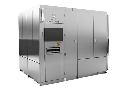
All units are contained within the panels, except the power supplies, cooling water circulator, and dry pump.
Table 1 Main specifications of JBX-8100FS (entry model)
| Items | JBX-8100FS(G1) Entry model |
|---|---|
| Acceleration voltage | 100 kV |
| Field size | 1,000 µm × 1,000 µm (HT), 100 µm × 100 µm (HR) (HT; High Throughput Mode / HR: High Resolution mode) |
| Minimum data increment | 0.5 nm (HT), 0.05 nm (HR) |
| Scan speed | 125 MHz |
| Scan speed modulation | 256 rank / resolution 0.05 nsec ~ |
| Positioning DAC / Scanning DAC | 20 bit / 14 bit |
| Beam diameter | 5.1 nm (HT), 1.8 nm (HR) |
| Minimum line width | <12 nm (HT), <8 nm (HR) |
| Field stitching accuracy | ≦ ± 20 nm (HT), ≦ ± 9 nm (HR) |
| Overlay accuracy | ≦ ± 20 nm (HT), ≦ ± 9 nm (HR) |
| Beam current stability | 0.2%p-p /h (@2 nA, HT) |
| Beam position stability | ≦ 60 nmp-p/h (@2 nA/HT), ≦ 10 nm/hp-p (@2 nA/HR) |
| Operating system | Linux, (‘Data preparation program’ can work on Windows 8.1 and 10) |
| Writing area | 150 mm × 150 mm |
| Substrate size | Full 6 inch wafer, 8 inch wafer loadable, small piece, 6 inch Mask |
| Maximum stage speed | 25 mm/sec |
| Laser measurement resolution | 0.6 nm |
| Electric requirements | 3 kVA (Main console 2 kVA, cwc 1 kVA, Normal) |
Other options include a 12 cassettes auto loading system and switchable acceleration voltage (50 kV/25 kV).
Performance Test Results
The performance of the JBX-8100FS with regard to minimum line width, field stitching accuracy, overlay accuracy and field in-plane dimensional accuracy was measured.
Minimum Line Width
To evaluate the lithography performance of the JBX-8100FS, a 50 nm thickness of ZEP520A resist (ZEON Corp.) was applied to a silicon substrate, and writing was performed under conditions of 100 pA beam current and a minimum beam diameter of 1.8 nm. A minimum line width of 8 nm or less is guaranteed. Special development was used this time to obtain an even finer structure. Low temperature development is generally known as a method for obtaining enhanced structures [1]. ZEP520A resist was developed at a temperature of 2.8°C, which allowed data demonstrating a minimum line width of 4.2 nm to be obtained (Fig. 2).
Fig.2 Cross section image of a minimum width line (×200 k)
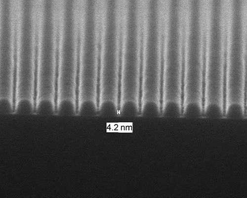
With ZEP520A (by ZEON) at thickness 40 nm, using the low-temperature effect, a line width of 4.2 nm can be achieved.
Field Stitching Accuracy
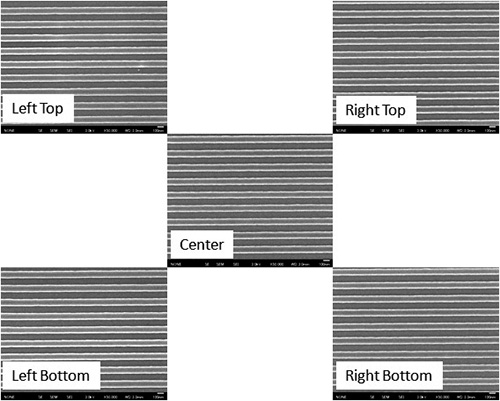
The JBX-8100FS utilizes a stage position correction system called Laser Beam Control (hereafter LBC), providing highly accurate position correction. Furthermore, with the addition of JEOL’s exclusive material distortion correction and deflection distortion correction, the accuracy is guaranteed. To measure the field stitching accuracy, an optical coordinate measurement system was used. "L" marks were placed at the corners of each processing field, and a 4 × 4 layout of fields was processed. The coordinates of the L-shaped marks at the points of intersection between the fields were measured, and the position accuracy was evaluated. The results for a 1000 μm area are reported here. The specifications guarantee an accuracy of within ± 20 nm or less. The actual results obtained were +11.5 nm / -9.8 nm (Fig. 3(a)). Even Vernier patterns with a resolution of 8 nm placed at the field corners were visually confirmed, and similar performance results were obtained (Fig. 3(b)).
Fig.3 Field stitching accuracy measurement results
(a) The measurement area was defined by a 4 × 4 array of points at 10 mm intervals (defining a 30 mm × 30 mm area), and the field stitching accuracy was measured. The guaranteed value is ± 20 nm or less, but the actual results obtained were +11.5 nm / -9.8 nm (X/Y).
(b) In the same way, the results of SEM observation of Vernier patterns with a resolution of 8 nm were obtained, and similar values were observed.
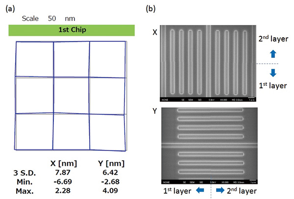
Overlay Accuracy
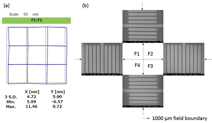
One feature of the SB is the ability to directly write a pattern onto a substrate which already has another pattern written on it. The EBL systems are equipped with a mark-detection function whereby alignment marks created on the material being processed can be detected and the coordinates determined. If the position of the pattern being drawn is recorded relative to the coordinates of the alignment marks, the deviation can be calculated and corrected when writing is performed. To evaluate this performance, EBL was used to process both the first and second layers. The writing area was 30 mm × 30 mm (4 × 4 points at 10 mm intervals.) The measurement was made by superimposing a 3 mm × 3 mm area (4 × 4 points at 1 mm intervals.) at one location within the 30 mm × 30 mm writing area, and the overlay accuracy was measured. The guaranteed performance is ± 20 nm or less, and the actual results obtained were +4.1 nm / -6.7 nm (Fig. 4(a)). Similarly, the results of measurements of Vernier patterns with a resolution of 8 nm showed that the superimposition was nearly perfectly centered in both the X and Y directions (Fig. 4(b)).
Fig.4 Overlay accuracy measurement values
(a) The writing area was defined by a 4 × 4 array of points at 10 mm intervals (defining a 30 mm × 30 mm area). The measurement area was defined by a 4 × 4 array of points at 1 mm intervals (defining a 3 mm × 3 mm area), and the overlay accuracy was measured. The guaranteed value is ± 20 nm or less, but the actual results obtained were +4.1 nm / -6.7 nm (X/Y).
(b) In the same way, the results of SEM observation of Vernier patterns with a resolution of 8 nm were obtained. For both the X and Y directions, the patterns were overlaid nearly at the center.
CD (Critical Dimension) uniformity within field
The drawing of a grating, like that required for DFB lasers, was performed and the accuracy of the line widths was determined. A line-and-space pattern was placed at the center and each corner of a 1000 μm field. Writing with a line width of 100 nm and 200 nm pitch was performed. The results show and accuracy of 1.1%p-p, with a maximum of 100.6 nm and a minimum of 99.5 nm (Fig. 5).
Fig.5 Critical dimension uniformity within field
A line-and-space pattern was placed at the center and each corner of a 1000 μm field. Writing with a line width of 100 nm and 200 nm pitch was performed. The results show and accuracy of 1.1%p-p, with a maximum of 100.6 nm and a minimum of 99.5 nm.
Stability
The stability is an important performance factor for EBL, which basically runs 24 hours per day. It is also possible to equip this system with a JEOL dedicated air conditioning unit and JEOL EMI countering unit, making it possible to achieve even better stability. The results of measurements in 100 kV High throughput mode using a current of 2 nA indicated a current drift of 0.08%p-p/h, and a beam position drift in the X direction of 9.5 nmp-p/h, and 10.8 nmp-p/h in the Y direction (Fig.6).
Fig.6 Stability
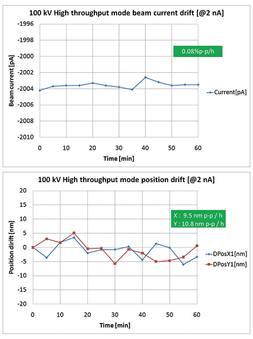
The stability was measured over a 1 hour period in 100 kV high throughput mode. Using a current of 2 nA, the current drift was 0.08%p-p/h, and the position drift in the X direction was 9.5 nmp-p/h, and 10.8 nmp-p/h in the Y direction.
Throughput
Since the beam profile is small with the SB, there is a tendency for the processing times to become longer in comparison to the variable type EBL. As mentioned above, since these are being used for manufacturing in recent years, the focus of device development has been on improving the throughput. The factors that determine the throughput of a lithography system include the stage movement time, stage settling time after movement, the correction time, data transfer time, the electrical system settling time, and the beam exposure time. The improvements in these factors achieved with the JBX-8100FS are described below.
- Stage movement time
This depends on the maximum speed of stage movement, but for short distances, the acceleration is also quite important. This has been improved by 10% to 20% through the optimization of the various parameters. - Data transfer time
This is the time needed for figure data transfer before writing. This has been improved to be 1/3 to 1/5 the time needed by conventional systems. - Sub Deflector Amplifier settling time
This is the time needed from data transfer until writing starts. Compared to the transfer time, this is now short enough to be ignored. - Beam exposure time
The beam irradiation time for a single spot with the spot beam, given by the following equation.

t: Beam irradiation time [sec], Q: Resist sensitivity [C/cm2], p: Shot pitch [cm], I: Beam current [A]
With the JBX-8100FS, the minimum value for t is 8 nsec (125 MHz when expressed as a frequency). Compared to conventional systems, scanning is possible at more than double the speed.
As a result of the improvements described above, a 30% to 40% improvement in the total writing time is possible for a pattern with a writing area covering about 10% of the total substrate surface.
Power Consumption
After a system is purchased, an important on-going factor becomes the running costs. Particularly for EBL systems, in order to obtain stable function, it is necessary to continuously supply the same electrical power, even when lithography is not being performed. The electrical units and power sections of the JBX-8100FS have been compactly designed, reducing the power consumption to 3 kVA during normal operation. This allows the system to be operated using only about 1/3 the power required by the conventional systems.
Summary
The R&D and production of semiconductor devices covers a broad range of applications, and the functions and precision required vary. The JBX-8100FS has been developed as an electron beam lithography system that can be used with high precision and high speed in any field, while also reducing power consumption. Future plans include further improvement of the throughput and improved substrate handling methods.
Acknowledgements
I would like to express my sincere appreciation to all the project members who provided advice and assistance with the development of this product.
References
- T. Okada, J. Fujimori, M. Aida, M. Fujimura, T. Yoshizawa, M. Katsumura, and T. Iida: "Enhanced resolution and groove-width simulation in cold development of ZEP520A" J. Vac. Sci. Technol. B 29 (2011) 021604.
Related Products
Are you a medical professional or personnel engaged in medical care?
No
Please be reminded that these pages are not intended to provide the general public with information about the products.