JBX-A9 Series
Electron Beam Lithography System

Features
High Precision and High Throughput Direct Writing System
Built with JEOL’s renowned Electron Optics for ultimate stability
Loadable wafer up to 300 mm
FOUP system optionally available
In-line extendibility to other process tools such as coaters and developers
Low power consumption
Improved ease-of-use for all experience levels
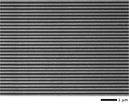
DFB Laser / Nanoimprint
Metalens
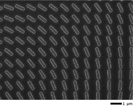
Lens Arrays
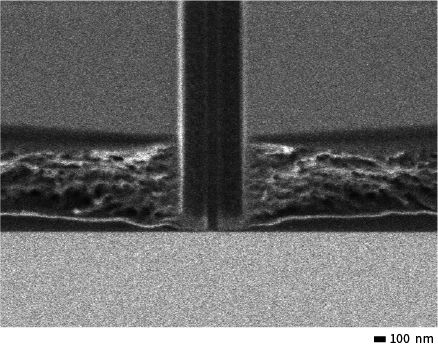
T-Gate
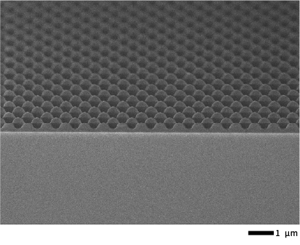
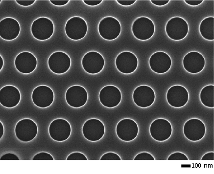
Photonic Crystal
Specifications
| Item | Specification |
|---|---|
| Accelerating Voltage | 100 kV |
| Maximum Field Size | 1000 μm |
| Minimum Increment | 0.25 nm |
| Stitching Accuracy | ±9 nm |
| Overlay Accuracy | ±9 nm |
| Minimum Line width | ≦8 nm |
| Beam Current | 50 pA to 400 nA |
| Maximum Scanning Speed | 200 MHz |
| Stage Positioning Resolution | 0.15 nm |
| Automatic Aberration Corrections | Dynamic Focus Dynamic stigmatism Deflection Distortion Correction |
| Maximum Sample Size | 300 Wafer 9 inch Mask |
| Power Consumption | 5 kVA |
| Footprint | 7.4 m × 5.3 m × 2.7 m (H) |
| Basic Configuration |
|---|
| Basic Unit |
| 10 Cassettes Auto Loading System |
| Control Program with CPU System |
| Additional License for Data Preparation Program |
| Remote Control OL Aperture |
| Options |
|---|
| in-situ Optical Microscope |
| FOUP Wafer Auto Loading System |
| Open Cassette 200 mm Wafer Auto Loading System |
| 48kV High Voltage Program |
| Custom Cassettes |
| SECS/GEM |
| Air Conditioner |
| EMI cancellation system |
* Contact local JEOL office for more details about other grade models.
Catalogue Download
JBX-A9 Series Electron Beam Lithography System
Application
Development of JBX-A9, Electron Beam Lithography System
Gallery


More Info
Are you a medical professional or personnel engaged in medical care?
No
Please be reminded that these pages are not intended to provide the general public with information about the products.