Development of JBX-A9, Electron Beam Lithography System
SE2024-01
JEOL NEWS Vol.59 No.1
Hiroshi Ozawa
SE Engineering Division, JEOL Ltd.
The JBX-A9 has been developed as a successor to the JBX-9500FS, a spot-beam electron beam lithography system. The JBX-A9 is a spot-beam e-beam lithography system for 300 mm wafers that inherits the basic specifications of the JBX-9500FS while achieving power and space savings, and is environmentally friendly through the use of a refrigerant-free chiller. With the field stitching accuracy within ±9 nm and overlay accuracy within ±9 nm, this system is suitable for applications that require particularly high beam positioning accuracy, such as photonic crystal device fabrication.
Introduction
Electron beam lithography systems enable fine patterning by irradiating an electron beam onto a material coated with resist that is sensitive to the electron beam and deflecting and scanning the beam. The history of electron beam lithography systems began in the 1960s, and development was promoted in the United States, Europe, and Japan [1]. In our company (Fig. 1), the first electron beam lithography system, JEBX-2A, was developed in 1966, and the following year, JEBX-2B, our first commercial electron beam lithography system, was born [2][3]. Subsequently, through advances in emitters (electron sources), the emergence of variable shaped-beam lithography systems, and the development of higher performance such as improved accelerating voltages and various correction techniques, multi-beam lithography systems are now in practical use [4]. Among them, the spot-beam type electron beam lithography system, which writes patters by scanning a
particularly narrowly focused electron beam, has a relatively simple hardware configuration similar to that of a scanning electron microscope. Nevertheless, this spot-beam system is used in a broad range of fields. These are covering the production of devices for optical communications such as DFB (Distributed FeedBack) lasers, the fabrication of micro periodic structures such as photonic crystals and metamaterials, the creation of optical elements such as optical waveguides and microlens arrays, and the fabrication of MEMS (Micro Electro Mechanical Systems) devices, the production of molds for nanoimprint lithography (NIL) equipment, Furthermore, the application fields of the spot-beam electron beam lithography system extend to the
research and development of next-generation devices such as two-dimensional materials (e.g. graphene) and quantum devices.
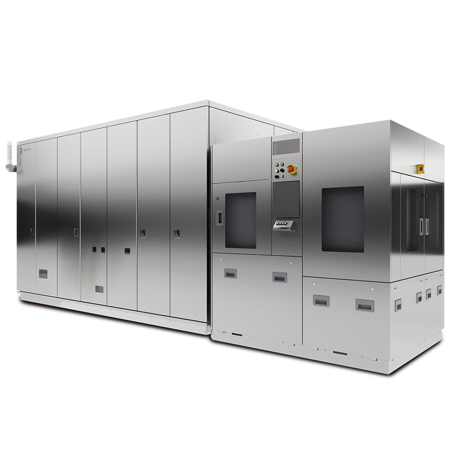
JEOL has developed the JBX-A9 (Fig. 2), a successor model of the JBX-9500FS, as a spot-beam electron beam lithography system for 300 mm wafers.
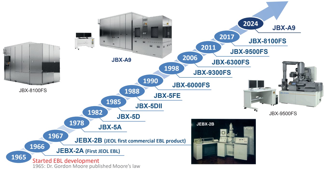
Fig. 1 Development history of JEOL spot-beam electron beam lithography systems.
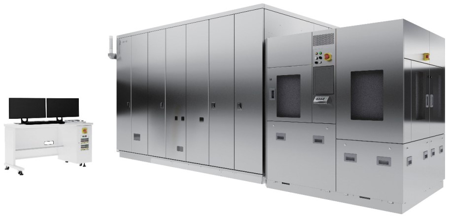
Fig. 2 JBX-A9 electron beam lithography system.
Development Concept
The JBX-A9, a spot-beam electron beam lithography system, inherits the basic specifications of the JBX-9500FS (predecessor of JBX-A9), and its development began as a 300 mm wafer-compatible system that achieves savings of power and space. Therefore, the mechanical units such as the column and stage, which are important elements for the performance of the lithography system, have been inherited from the JBX-9500FS. On the other hand, the electrical control unit is the same as JBX-8100FS or uses the same design concept to reduce the number of control racks, thereby reducing size and power consumption. As a result, the JBX-A9 consumes less than half the power of the JBX-9500FS and also has a reduced footprint of about 1/3 (Table 1). In addition, the JBX-A9 has an enclosure covering the electron optical column, exposure chamber, and various control units. This design was hinted by the JBX-8100FS. The entire unit is covered for a clean appearance, and the temperature inside the enclosure can be stabilized by connecting an air conditioner. However, unlike the JBX-8100FS, the operator’s control unit works as a separate control console that can be rearranged to suit the installation room, as in the case of the JBX-9500FS.
Among the electrical control units of the JBX-A9, the unit that controls the main deflector (DEF AMP: deflector amplifier) is available in two types: a high-precision deflection system developed based on the unit installed in the JBX-9500FS and a deflection system common to the unit installed in the JBX-8100FS, allowing customers to select and configure one of them according to their needs and budget.
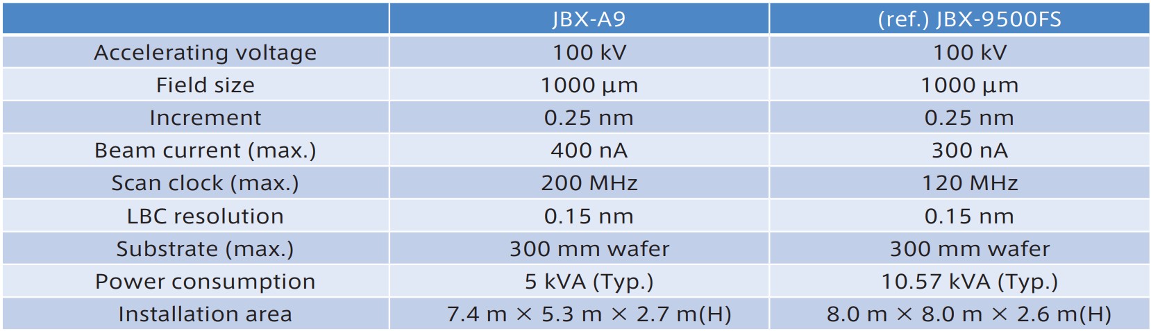
Table 1 Main specification of the JBX-A9.
Features of JBX-A9
The name “A9” differs significantly from the combination of four digits and two letters used in our recent spot-beam e-beam lithography systems, such as the 9500FS and 8100FS. In considering a successor model to the JBX-9500FS, we held internal discussions to create an abbreviation that would appeal strongly to our customers, especially overseas users, and to make it easier to call the new model, which led to the adoption of the simple model name A9, which is a return to the basics. The “A” in A9 stands for “Accurate”, “Automatic”, and “Advanced”. The “9” indicates that this is a top-of-the-line model in the same vein as the JBX-9300FS and JBX-9500FS. Hereinafter, we will explain the features of the JBX-A9 using these three “A” as keywords.
Accurate
The main performances of the JBX-A9 are listed in Table 2.
One of the important performance indicators of an electron beam lithography system is the field stitching accuracy. The field is the area that can be drawn by deflecting the beam with the deflector while the stage is stationary. In the writing method called the step-and-repeat method (Fig. 3), which alternately combines writing within this field and stage movement to write a wide area, as the smaller the stitching error between the fields is, the lithography performance is better. In addition, it is sometimes requested to write a pattern at a desired position by positioning it in line with a substrate pattern that already exists on the material. The JBX-A9’s field stitching accuracy and overlay accuracy are both within ±9 nm. The high-precision stage and laser beam control (LBC) system are indispensable to achieve this accuracy.
The cassette loaded with a writing material is transferred onto a stage, and this stage moves on the XY plane to write over a wide area on the writing material. Therefore, the accuracy of the stage affects the aforementioned stitching and overlay accuracy of the writing fields. Therefore, the JBX-A9 stage uses a high-precision stage with a mechanism that has a proven track record in the JBX-9500FS. This stage was originally developed for use in mask lithography systems and has been adapted for use in spot beam lithography systems. To control the beam position with high precision, the electron beam lithography system uses a laser interferometer position measurement system to measure the stage position and correct the beam irradiation position by deflecting the electron beam by a distance equivalent to the error from the target position. The measurement resolution is as fine as about 0.15 nm in the case of JBX-A9 (Fig. 4).
One application that requires highly precise control of the beam irradiation position is photonic crystal devices. Photonic crystals are periodic structures close to the wavelength of light, and by precisely controlling their periodicity, it is possible to confine and amplify light. Microfabrication technologies such as electron beam lithography systems are used to fabricate these periodic structures. However, since the patterning accuracy directly affects device performance, it is necessary to write the pattern precisely at the desired location. The JBX-9500FS has a proven track record in the fabrication of photonic crystals and thus, the photonic crystal will be one of the key applications for the JBX-A9.
Table 2 Main performances of the JBX-A9.
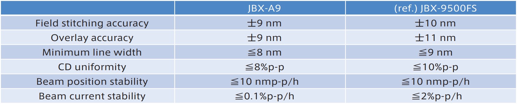
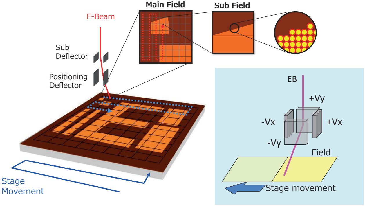
Fig. 3 Electron beam lithography by the step-and-repeat method.
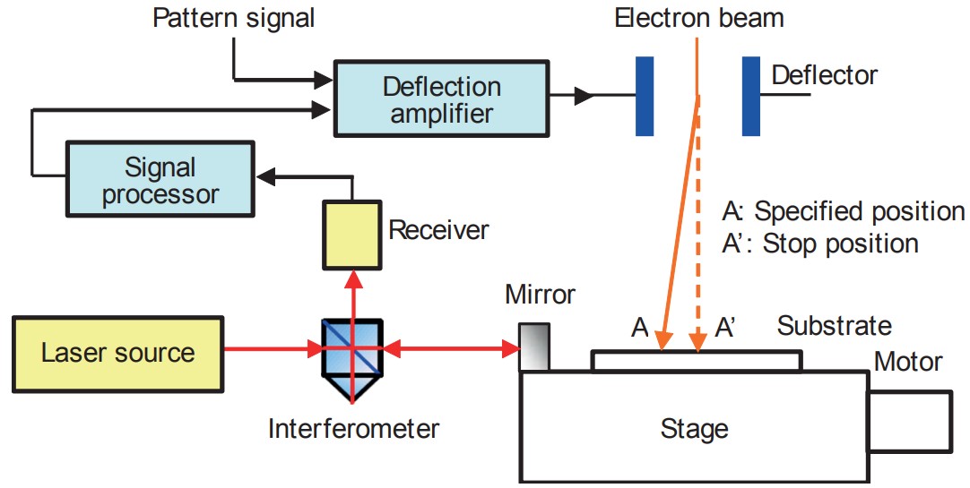
Fig. 4 Correction of the electron beam irradiation position by the laser interferometer position measurement system.
Automatic
The JBX-A9 has a cassette transfer system capable of continuously and automatically transferring up to 10 cassettes (Fig. 5). Cassettes stored in the stocker are automatically loaded onto the stage based on the writing job specifications, and when writing is finished, they are unloaded from the stage and stored in the stocker again. Even when writing conditions, such as beam current, are different, the electron optical system is automatically reconfigured and the position of the objective aperture is adjusted according to the writing job specifications. Of course, it is also possible to stop writing in the middle of a job or to modify the writing order (called the writing queue) to continue operation.
Several new or improved features for automatic adjustment of the electron optics system has been added, and when used in conjunction with the Python scripts that come standard with the JBX-A9, a series of writing-related operations can be executed at the intentions of users.
Furthermore, by replacing the cassette transfer system section with a wafer transfer system, the specifications allow for the continuous automatic transfer of up to 25 wafers as a 300 mm FOUP-compatible carrier mode, or the full automation of resist coating, writing, and pattern-developing in an in-line mode by connecting with a coater/developer from another manufacturer.
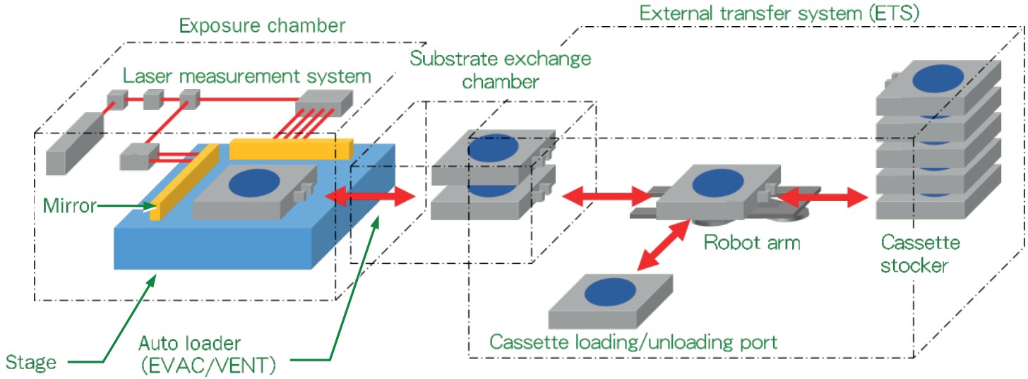
Up to two cassette stockers (total: 10 cassettes) are loadable.
Fig. 5 Cassette transfer system.
Advanced
The optical microscope, which has been available as an option since the JBX-8100FS, is a unique feature that allows the user to check the surface of the writing material in the exposure chamber without using an electron beam, but it has the limitation that the observed area is limited. To overcome this problem, the JBX-A9 is fitted with two optical microscopes and seamlessly switches between two optical microscope images according to the stage position, making it possible to observe the entire writable area. This feature is useful, for example, when searching for marks or objects to be written on the material, as SEM images are irradiated with an electron beam on the material surface, which sensitizes the resist, whereas optical microscope images can be used to search for marks or objects to be writing without sensitizing the resist.
Let us take the case of fabricating electrode patterns on a substrate with scattered graphene flakes (Fig. 6). Graphene flakes vary in size and shape, and their location on the substrate cannot be determined without actual observation. Therefore in the past, before placing the material in the lithography system, the position of the flakes was checked with an optical microscope, and the coordinates were identified from the marks
placed on the material in advance, then the pattern was written with the lithography system based on this information. The JBX-A9 can immediately reflect the coordinate values in the writing job immediately after the object is found in the optical microscope image, thus greatly improving work efficiency.
In conjunction with the development of the JBX-A9, a new pattern data format, JEOL53, was also developed for spot-beam electron beam lithography systems. This format extends the conventional JEOL52 (V3.0) format by adding rotated rectangle and rotated trapezoid elements with arbitrary angles, and is expected to improve a line edge roughness (LER) and a finishing uniformity, especially in the representation of circles and curves (Fig. 7). Furthermore, compared to the conventional method of expressing curves using only rectangles and trapezoids, this function reduces the number of figures, thereby reducing data volume, and it also improves the writing throughput by reducing the various settling times that are generated depending on the number of figures. This function is optionally applicable to JBX-8100FS and JBX-9500FS, but is standard on the JBX-A9.
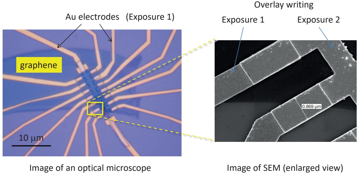
Samples and images courtesy of Graphene Research Centre, National University of Singapore.
Fig. 6 Fabrication of electrode patterns on graphene.
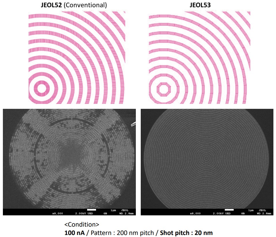
Pattern writing was executed with large beam current and rough shot pitches, which causes large difference in the writing results.
Fig. 7 Comparison of writing results by difference in data format.
Environmental Consideration (Consciousness)
In recent years, there has been a growing awareness of the environmental burden, and environmental consideration has become an indispensable factor in the development of equipment. In electron beam lithography systems, cooling water is circulated to cool the heat-generating parts and to stabilize the temperature of the system. Hydrofluorocarbons (HFCs) used as refrigerants in this cooling water circulation system have an extremely high global warming potential (GWP), and there is a need to reduce HFCs and switch to low-GWP refrigerants. To achieve this goal, the JBX-A9 uses a Peltier-cooling water circulation system that does not use refrigerants. This reduces the burden of users for daily inspections and legal regulations at time of disposal. The fact that the JBX-A9 is environmentally friendly is a major appealing point at the time of equipment selection by the user.
Summary
We have introduced the JBX-A9, a spot-beam electron beam lithography system. This new system inherits the basic performance of the JBX-9500FS while saving power and space, and is also environmentally friendly through the use of a refrigerant-free chiller. The JBX-A9 is expected to be used in various fields as a top-of-the-line spot-beam electron beam lithography system.
Acknowledgements
The project to develop this equipment kicked off in January 2019, but was subsequently forced to revise its original plan due to changes in work styles caused by the global spread of new COVID infections and subsequent manufacturing difficulties due to tight materials. Nevertheless, the fact that we were able to overcome these difficulties and bring a new product to the market is owing to the efforts of the project members and all other parties involved. I would like to take this opportunity to express my deepest gratitude.
References
[ 1 ]Semiconductor History Museum of Japan. “1970s Electron Beam Lithography System ~ Equipment & Materials Table of Contents ~”. 2022-05-11.
[ 2 ]S. Miyauchi, et al. “Electron Beam Lithography”, Journal of the Vacuum Society of Japan. 12(7) 1969.07,p.250~258. (in Japanese).
[ 3 ]K. Kazato, “Let us push forward with Electron Microscopes! (last volume)”, Nihon-Tosho-Kankoukai, 2004.12. 4-8231-0789-6,p.320~327. (in Japanese).
[ 4 ]Christof Klein, and Elmar Platzgummer, “MBMW101: World’s 1st High-Throughput Multi-Beam Mask Writer”, Proc. SPIE Vol. 9985, 998505-7 (2016).
Solutions by field
Related products
Are you a medical professional or personnel engaged in medical care?
No
Please be reminded that these pages are not intended to provide the general public with information about the products.