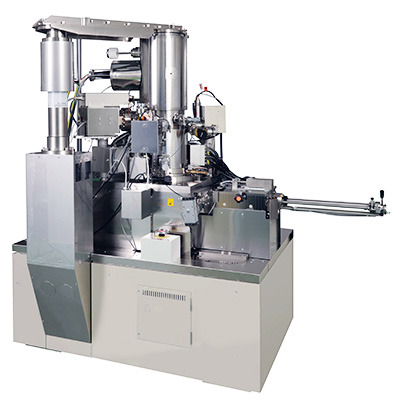
【DISCONTINUED】JBX-6300FS Electron Beam Lithography System
DISCONTINUED
This product is no longer available.
If you would like to know the latest information about your preferred product or to find out more about alternatives, please click on the link below. We hope you will continue to use our products.
JBX-6300FS can easily write patterns down to 8nm or less (actual result: 5nm) by the employment of an electron optical system that automatically adjusts a 2.1nm-diameter electron beam at 100kV accelerating voltage. Furthermore, this EB system achieves high field-stitching and overlay accuracy of 9nm or less, providing high cost performance. Furthermore, a unique automatic correction function developed by JEOL enables high-precision pattern writing. JBX-6300FS responds to a wide range of requirements, such as R&D of cutting-edge devices, nanotechnology-related R&D and communication-device production.
Features
JBX-6300FS can write highly precise patterns even at field corners and boundaries by the use of its powerful electron optical system that automatically corrects distortions generated by beam deflection.
Since JBX-6300FS has a high-precision stage that employs Beam positioning DAC of 19bits with 0.125nm resolution and Laser interferometer with 0.6nm resolution, the top-of-the-line writing positional accuracy of 9nm or less is achieved for small fields to large-area fields.
JBX-6300FS has an automatic beam adjustment function, enabling beam-dose correction and beam-position correction during pattern writing.
Timing of correction can be set for each field or each pattern. This function is very effective for a long period writing without an operator, for example at weekends or consecutive holidays.
JBX-6300FS dramatically shortens pattern-writing time because of its high scan speed up to 50MHz and also because the machine overhead time is reduced as much as possible. Operations until the start of writing are very simple as well as automatic focusing, thus enhancing the total throughput.
If the Auto Loader (option) is employed, JBX-6300FS can perform continuous writing for the specimen holders up to 10. (Ex: continuous writing up to 10 wafers of 150mmφ, up to 40 wafers of 50mmφ, etc. ※To perform continuous writing, the sample holders equivalent to the number of materials). JEOL has delivered such an EB system to production lines in Japan and overseas.
The use of Fine Pitch Control Program (field size fine modulation program) enables JBX-6300FS to fabricate a chirped-period grating such as a DFB laser.
Introduction results
Over more than 40 years, JEOL has delivered a great deal of EB systems to research institutions and production lines in Japan and overseas.
Specifications
| Electron gun | ZrO/W Shottky type |
|---|---|
| Writing method | Spot beam, Vector scan, Step & repeat |
| Acc. Voltage | 25kV (option), 50kV, 100kV |
| Material size | Up to 200mmΦ wafer, Up to 5-inch or 6-inch mask, Micro sample of any size |
| Maximum field size | 2000μmX2000μm |
| Stage movement range | 190mmX170mm |
| Overlay accuracy | ≦±9nm |
| Field stitching accuracy | ≦±9nm |
| Scan speed | Up to 50MHz |
More Info
Are you a medical professional or personnel engaged in medical care?
No
Please be reminded that these pages are not intended to provide the general public with information about the products.