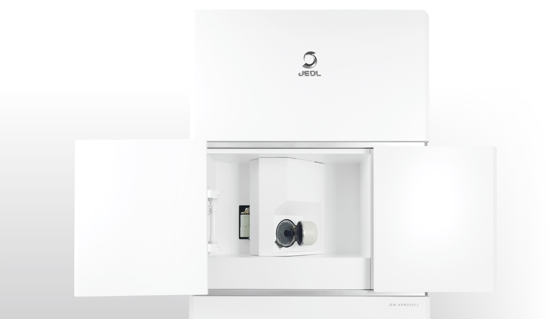
JEM-ARM300F2
GRAND ARM™2 Atomic Resolution
Analytical Microscope
A New Atomic Resolution Electron Microscope has been released!
The "GRAND ARM™2" has been upgraded.
This new "GRAND ARM™2" enables observation at ultrahigh spatial resolution with highly sensitive analysis over a wide range of accelerating voltages.
Features
Feature1
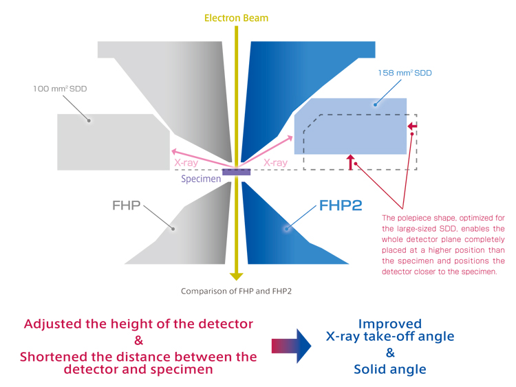
FHP2 newly developed objective lens pole-piece
The FHP objective lens pole piece is optimized for ultrahigh spatial resolution observation.
While maintaining this capability, the shape of the pole piece was further optimized for X-ray solid angle and take-off angle of the large-sized Dual SDDs (158 mm2).
As the result, the effective X-ray detection efficiency of the FHP2 is more than twice as sensitive as that of the FHP. It can provide sub-angstrom resolution in EDS elemental maps.
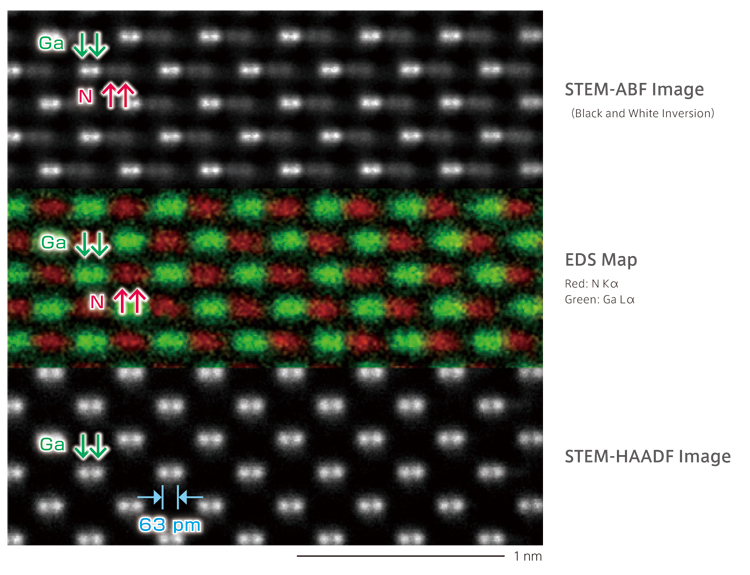
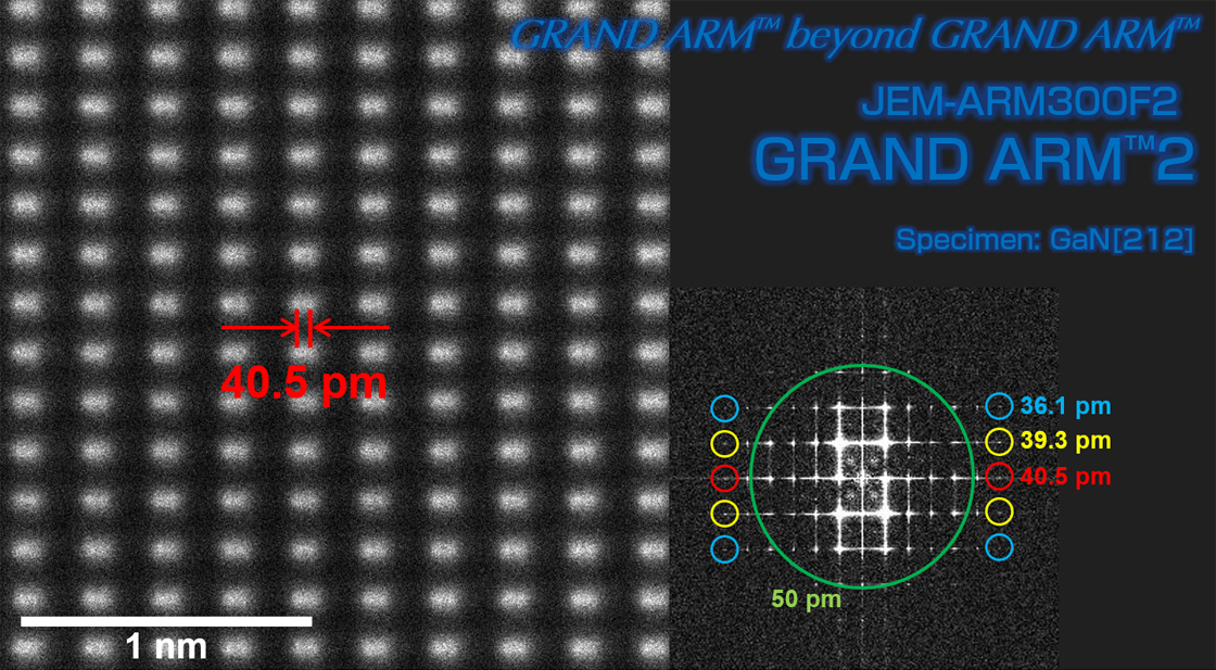
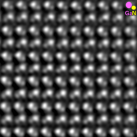
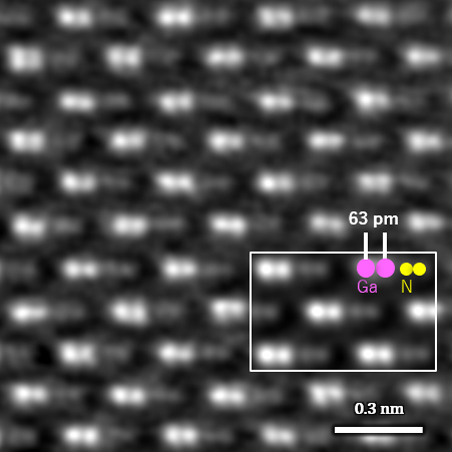
Atomic resolution STEM-HAADF/ABF images and EDS maps for GaN[211]
Feature2
New enclosure
The TEM column is covered by a box-type enclosure, which can reduce the effect of environmental changes such as temperature, air flow, acoustic noise and so on, and then it improves the stability of microscope.
Feature3
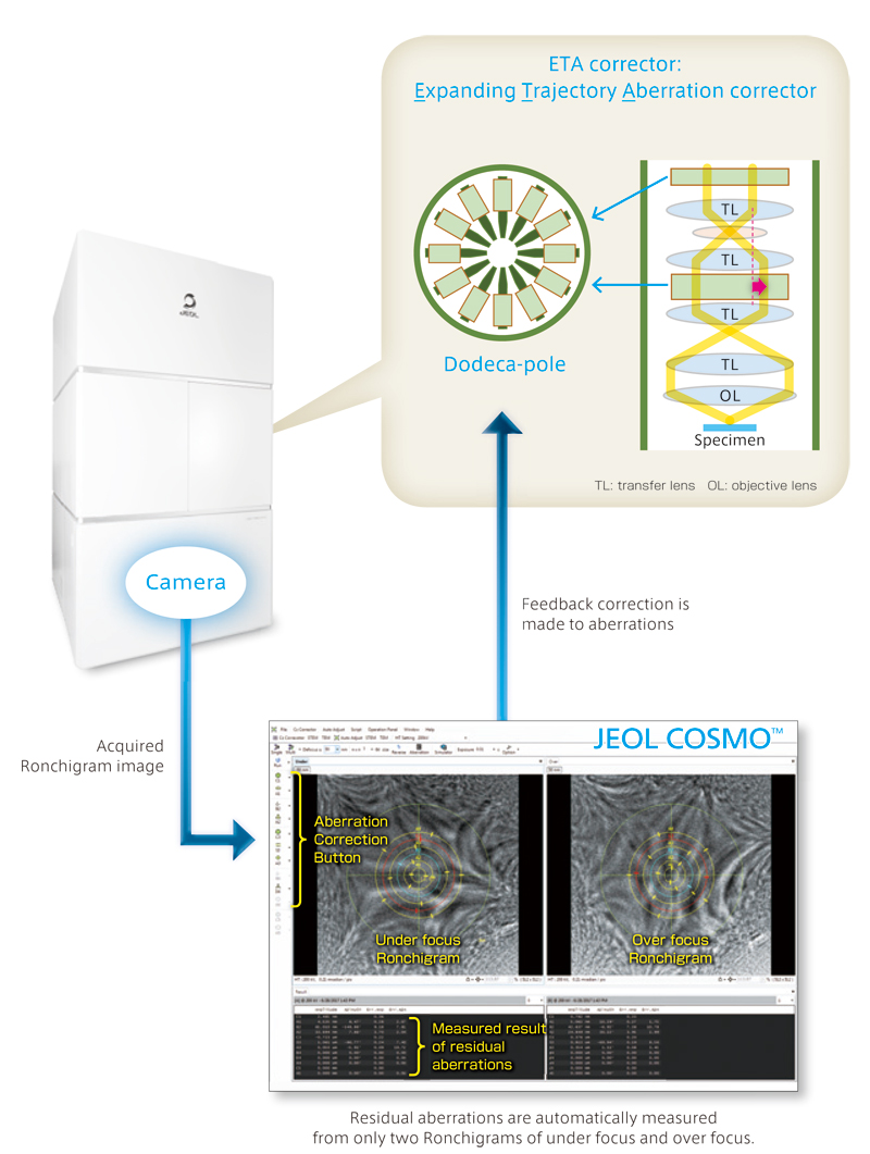
ETA corrector & JEOL COSMO™
Quick & Accurate aberration correction
JEOL COSMO™ uses only 2 Ronchigrams acquired from any amorphous area to measure and correct aberrations.
Therefore, the system can provide Quick and Accurate aberration correction without dedicated specimens.
Feature4
Improvement of stability
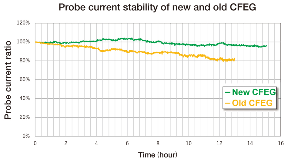
New CFEG (Cold Field Emission electron Gun) adopted a smaller SIP with a larger evacuation volume than before for GRAND ARM™2. Enhancement of evacuation volume of SIP improves the degree of vacuum near the emitter inside CFEG, and also improves the stability of emission and probe currents. The miniaturization of SIP can reduce the total mass of CFEG by ~100 kg.
The weight saving of CFEG improves resistance to vibration for the microscope.
Other improvements also enhance the stability and resistance to various disturbance for the microscope.
| Acceleration voltage | GRAND ARM™ (FHP) | GRAND ARM™2 (FHP2) |
|---|---|---|
| 300 kV | 63 pm | 53 pm |
| 200 kV | 78 pm | 63 pm |
| 80 kV | 136 pm | 96 pm |
| 60 kV | 136 pm | 96 pm |
| 40 kV | 192 pm | 136 pm |
| Acceleration voltage | GRAND ARM™ (WGP) | GRAND ARM™2 (WGP) |
|---|---|---|
| 300 kV | 82 pm | 59 pm |
| 200 kV | 105 pm | 82 pm |
| 80 kV | 136 pm | 111 pm |
| 60 kV | 192 pm | 136 pm |
| 40 kV | 313 pm | 192 pm |
Table 1. Guaranteed STEM image resolution with STEM ETA corrector for GRAND ARM™ and GRAND ARM™2.
Feature5
OBF System (Option)
In the new imaging method 'OBF STEM (Optimum Bright Field STEM)', raw images acquired by a segmented STEM detector are used as the source for a phase image reconstruction, with dedicated Fourier filters to maximize the signal to noise ratio of retrieved image.
This promising method realizes higher contrast for both heavy and light elements even while operating under extremely low electron dose conditions. Beam sensitive materials difficult to observe with standard ADF and ABF STEM methods can be easily analyzed with higher contrast at a wide range of magnifications.
K. Ooe, T. Seki, et al., Ultramicroscopy 220, 113133 (2021)
STEM Low Dose Imaging
The beam sensitive materials including Metal Organic Frameworks (MOFs) and Zeolites require a reduced electron dose (typically, probe current < 1.0 pA) while maintaining clear atomic contrasts for the framework of light elements.
The OBF STEM has an advantage for such low dose experiments, realizing ultra high dose-efficient STEM imaging in an atomic resolution.
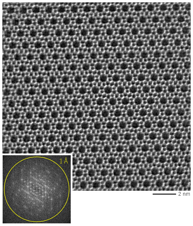
Both of OBF STEM Image MOF MIL-101(left) and MFI Zeolite (right) are acquired in a single shot and the high spatial resolution of 1 Å can also be observed on the FFT pattern in right inset. Moreover, stack image averaging (left inset) confirms that resolution and contrast are very well balanced.
Sample : MOF MIL-101
Instrument : JEM-ARM300F2
Accelerating Voltage : 300 kV
Convergence Semi-angle : 7 mrad
Probe current : < 0.15 pA
Insets) FFT pattern and 50 frames averaged image
Sample courtesy of Prof. Zhenxia Zhao, Guangxi University
Sample : MFI Zeolite
Instrument : JEM-ARM300F2
Accelerating Voltage : 300 kV
Convergence Semi-angle : 16 mrad
Probe current : 0.5 pA
Insets) FFT pattern
High Contrast Imaging for Light Elements
In addition to being highly dose efficient, OBF STEM is also advantageous for light element imaging.
Even in a lower acceleration voltage, both higher contrast and spatial resolution can be achieved for light elements.
Sample : GaN [110]
Instrument : JEM-ARM200F
Accelerating Voltage : 60 kV
Convergence Semi-angle : 35 mrad
Sample : Graphene
Instrument : JEM-ARM200F
Accelerating Voltage : 60 kV
Convergence Semi-angle : 35 mrad
The resolution for light elements becomes much better with a higher acceleration voltage.
Each atomic column is now clearly separated with a deep sub-angstrom resolution inside complex structures or along higher-index crystallographic axes.
The quality of OBF STEM is excellent in low dose conditions, and further enhanced under the standard probe conditions of a Cs-corrected electron microscope.
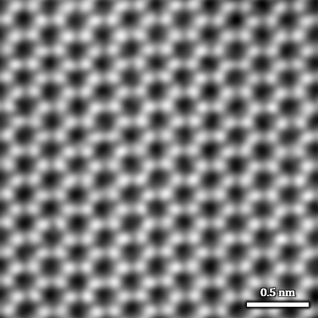
Sample : β-Si3N4 [0001]
Instrument : JEM-ARM200F
Accelerating Voltage : 200 kV
Convergence Semi-angle : 24 mrad
Inset) 10 frames averaged
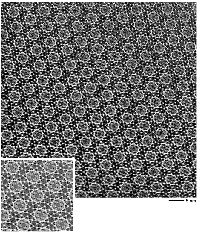
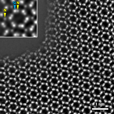
Sample : GaN [211]
Instrument : JEM-ARM300F2
Accelerating Voltage : 300 kV
Convergence Semi-angle : 32 mrad
Inset) 20 frames averaged
e-ABF (enhanced ABF) is not available in SAAF Quad configuration.
Live OBF Imaging
In an actual experiment, live OBF imaging is fundamental for beam sensitive materials as all operations should be performed in a dose limited condition. The live function is included in the OBF system, implemented within the TEM control software, with simple GUI control and real time display updates alongside conventional STEM images.
Movie
Live observation of OBF-STEM images with JEM-ARM200F
◆Click the "replay" button in the box above, and the movie will start (about 1 min.) ◆
Link
News Release
Specifications
Main Specifications
| Version | Ultra-high resolution configuration | High resolution configuration |
|---|---|---|
| Objective lens polepiece | FHP2 | WGP |
| Standard Accelerating Voltage | 300kV, 80kV | |
| Electron gun | Cold field emission gun | |
| STEM Resolution | 300kV / 80kV STEM Cs corrector installed | |
| 53 pm / 96 pm | 59 pm / 111 pm | |
| TEM Resolution | 300 kV / 80 kV TEM Cs corrector installed | |
| Lattice resolution 50pm / - | Lattice resolution 60 pm / - | |
| Non-linear information limit
60 pm / 90 pm |
Non-linear information limit
70 pm / 100 pm |
|
| Linear information limit
90 pm / 160 pm |
Linear information limit
100 pm / 170 pm |
|
| Maximum tilt angle | When using JEOL specimen tilting holder for analyses | |
| X:± 30°/ Y:± 27° | X:± 36°/ Y:± 31° | |
| When using High tilt specimen holder | ||
| X:± 90° | X:± 90° | |
Catalogue Download
JEM-ARM300F2 GRAND ARM™2 Atomic Resolution Analytical Microscope
Application
Application JEM-ARM300F2
Gallery
EDS Gallery
Cerium(IV) Oxide nano particle (Mn-doped)
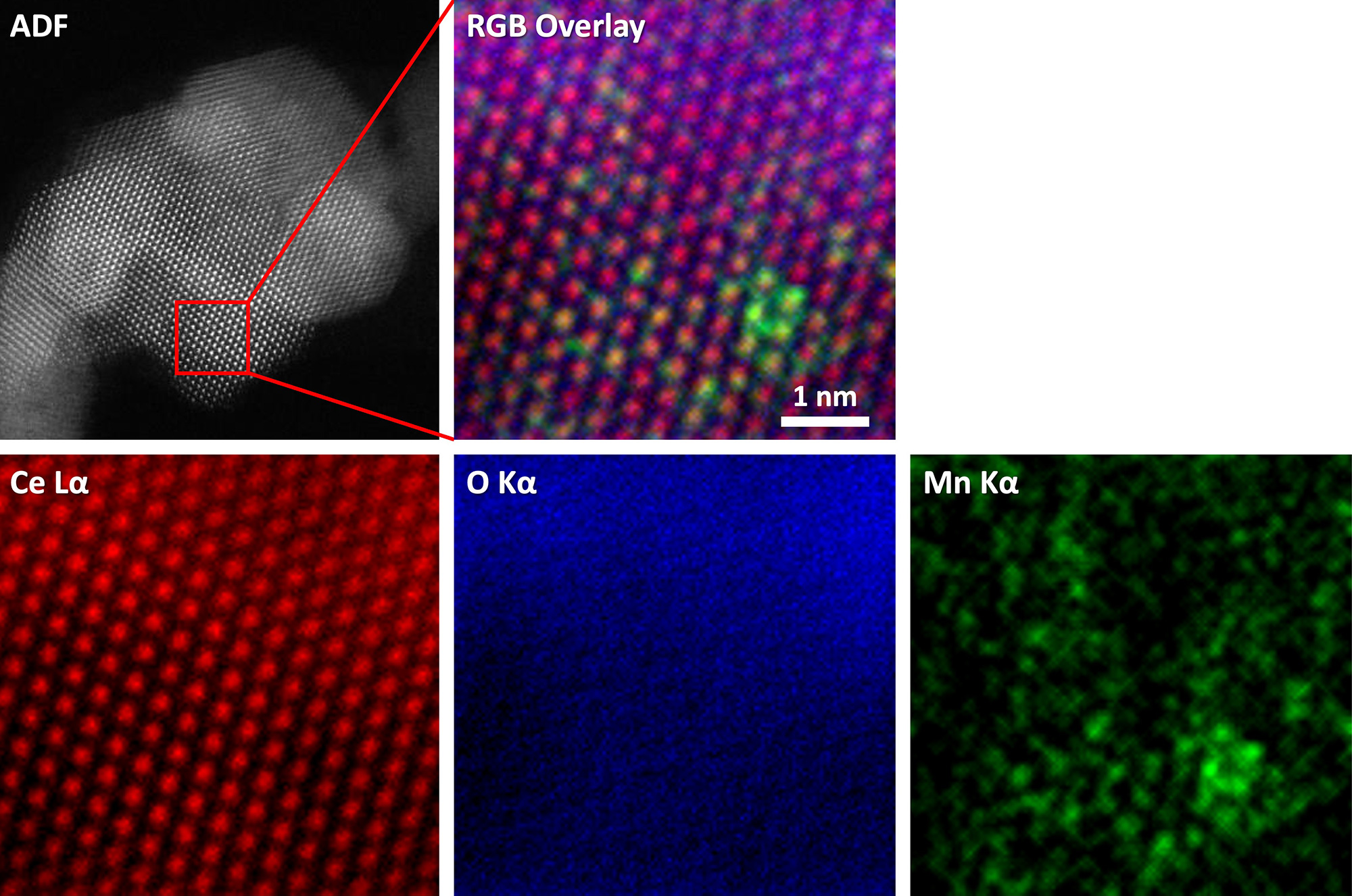
Image filtering applied
| Sample | Cerium(IV) Oxide nano particle(Mn-doped) |
|---|---|
| Acc. voltage | 300 kV |
| Probe current | ~27 pA |
| Map size | 128×128 pixel |
MnAl-Garnet
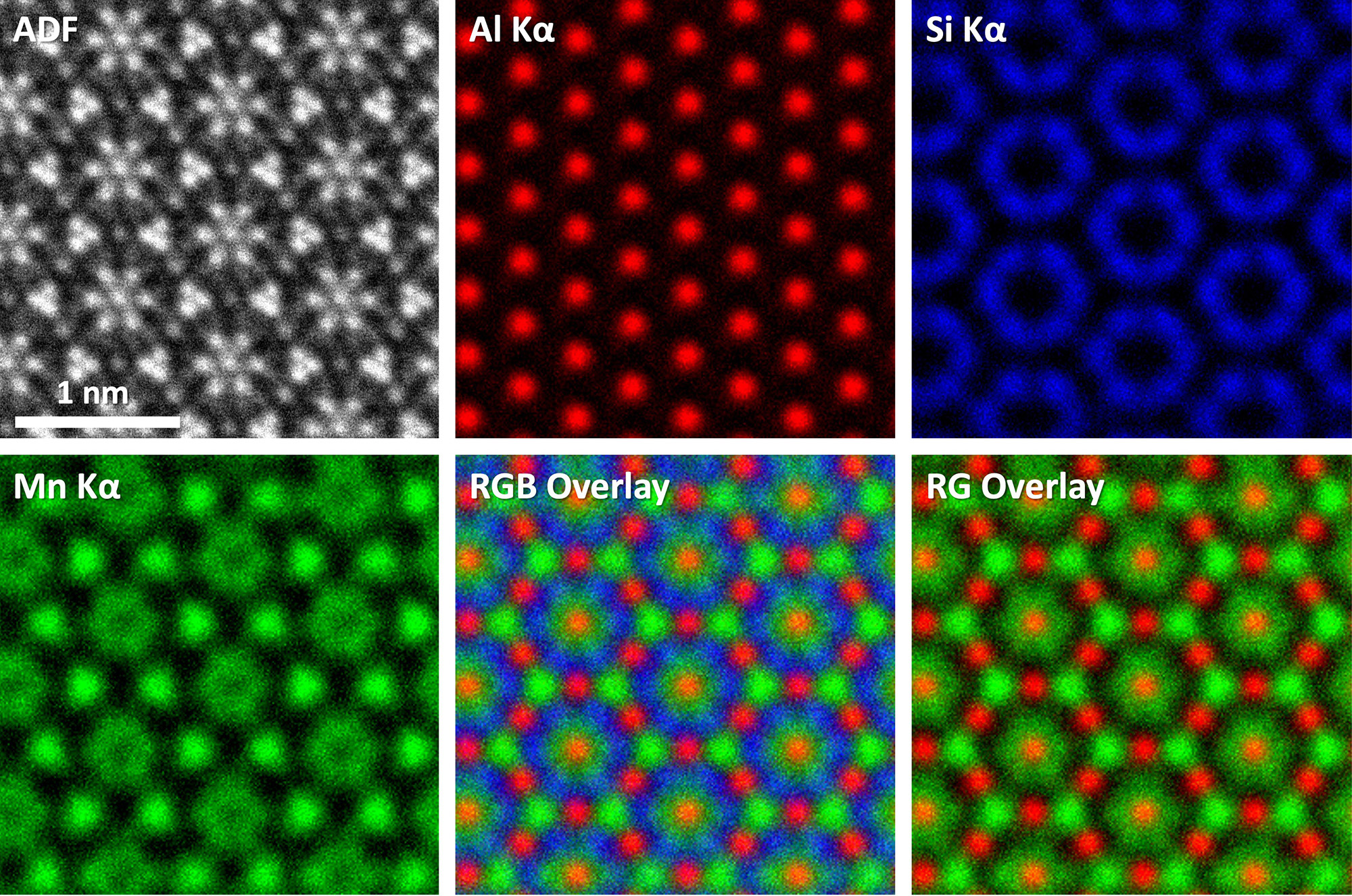
Image filtering applied
| Sample | MnAl-Garnet |
|---|---|
| Acc. voltage | 300 kV |
| Probe current | 12 pA |
| Map size | 256×256 pixel |
CaMg-Pyroxene
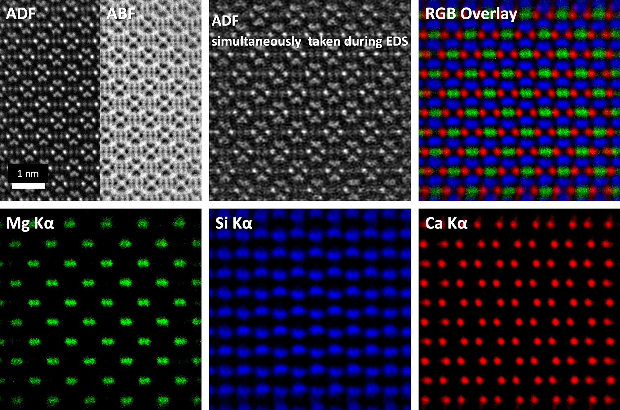
Image filtering applied
| Sample | CaMg-Pyroxene |
|---|---|
| Acc. voltage | 300 kV |
| Map size | 256×256 pixel |
The Interface between CaFe-Pyoxene and CaMg-Pyroxene
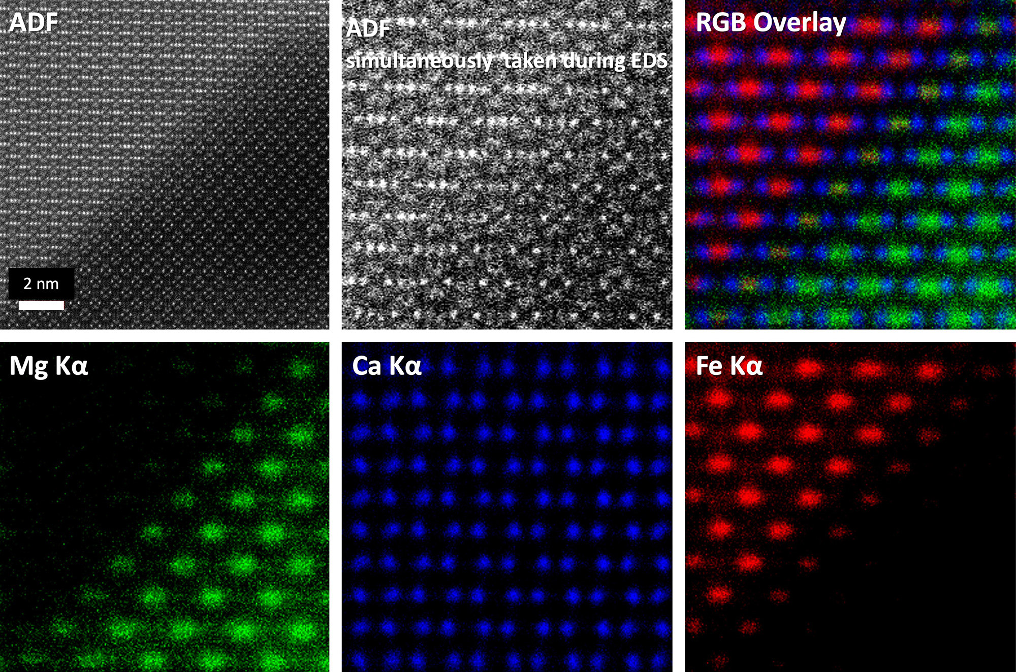
Image filtering applied
| Sample | CaFe-Pyoxene/CaMg-Pyroxene |
|---|---|
| Acc. voltage | 300 kV |
| Map size | 256×256 pixel |
Movie
JEOL Atomic resolution EDS map by GRAND ARM™2 with FHP2 pole piece and 158mm2 dual SDD system
◆Click the "replay" button in the box above, and the movie will start (about 1 .5min.) ◆
Related Products
SightSKY™ Series High-Sensitivity, Low-Noise Fiber-Coupling CMOS Camera
High-sensitivity, low-noise 19 M pixel CMOS sensor enables imaging of fine specimen detail and obtains high signal to noise images even at low electron doses.A Global shutter and high frame rate (58 fps/full pixel mode) enable image series acquisitions with less artifacts during in-situ dynamic observation studies.The SightSKY™ camera system offers integration with JEOL’s FEMTUS™ Integrated Analysis Platform, providing user-friendly operation and data acquisition.
More Info
Are you a medical professional or personnel engaged in medical care?
No
Please be reminded that these pages are not intended to provide the general public with information about the products.