JSM-IT510
InTouchScope™ Scanning
Electron Microscope
 Powered by Bioz
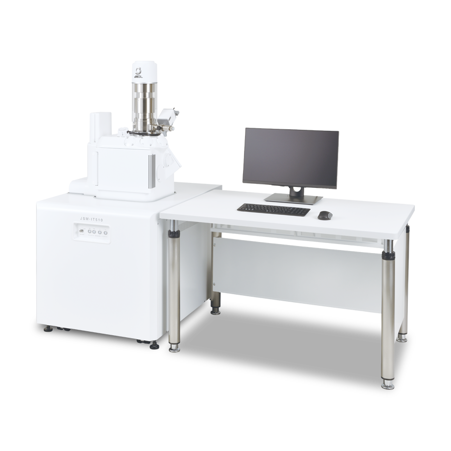
Easy to acquire data for all specimen types
Scanning electron microscopes (SEMs) are indispensable tools not only for research but also for quality assurance and manufacturing sites.
At those scenes, the same observation processes need to be performed repeatedly and there has been a need to improve the efficiency of the process.
With the JSM-IT510, the newly added Simple SEM function allows users to "leave the manual repetitive operation to it", required for SEM observation, making SEM observation more efficient and easier.
Features
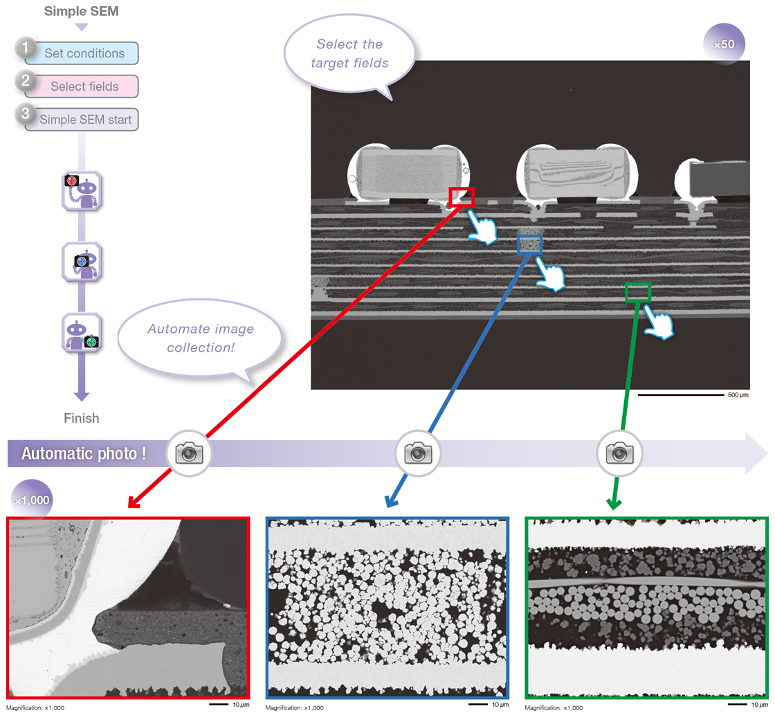
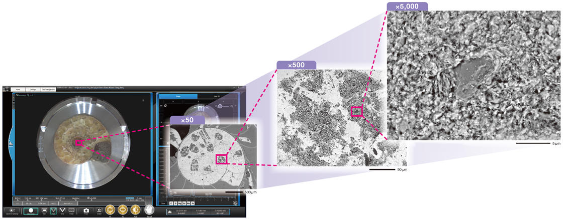
Simple SEM
Just select the target field
Simple SEM supports daily routine work.
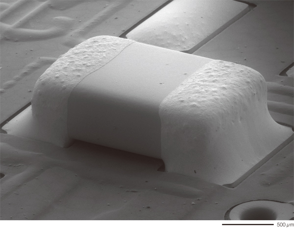
Specimen: Electronic device
Accelerating voltage: 15 kV, (Top) Magnification: ×50 (Bottom) ×1,000, Signal: BE
Video introducing the JSM-IT510
Functions of Simple SEM are introduced.
◆Clicking the Play button starts the video (approx. 2 minutes).
Specimen Exchange Navi
Guide from specimen exchange to automatic observation
Safe and simple! Specimen Exchange Navi
1. Follow the Navi guide to set specimen
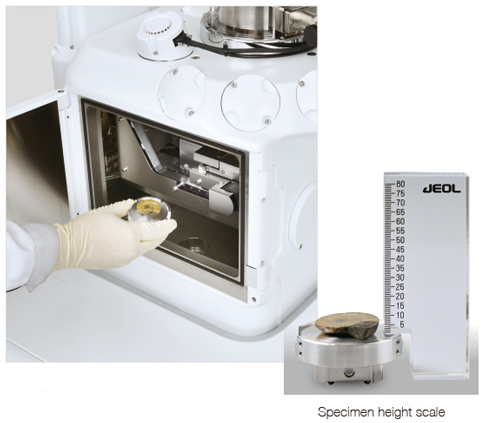
2. Prepare for observation during evacuation
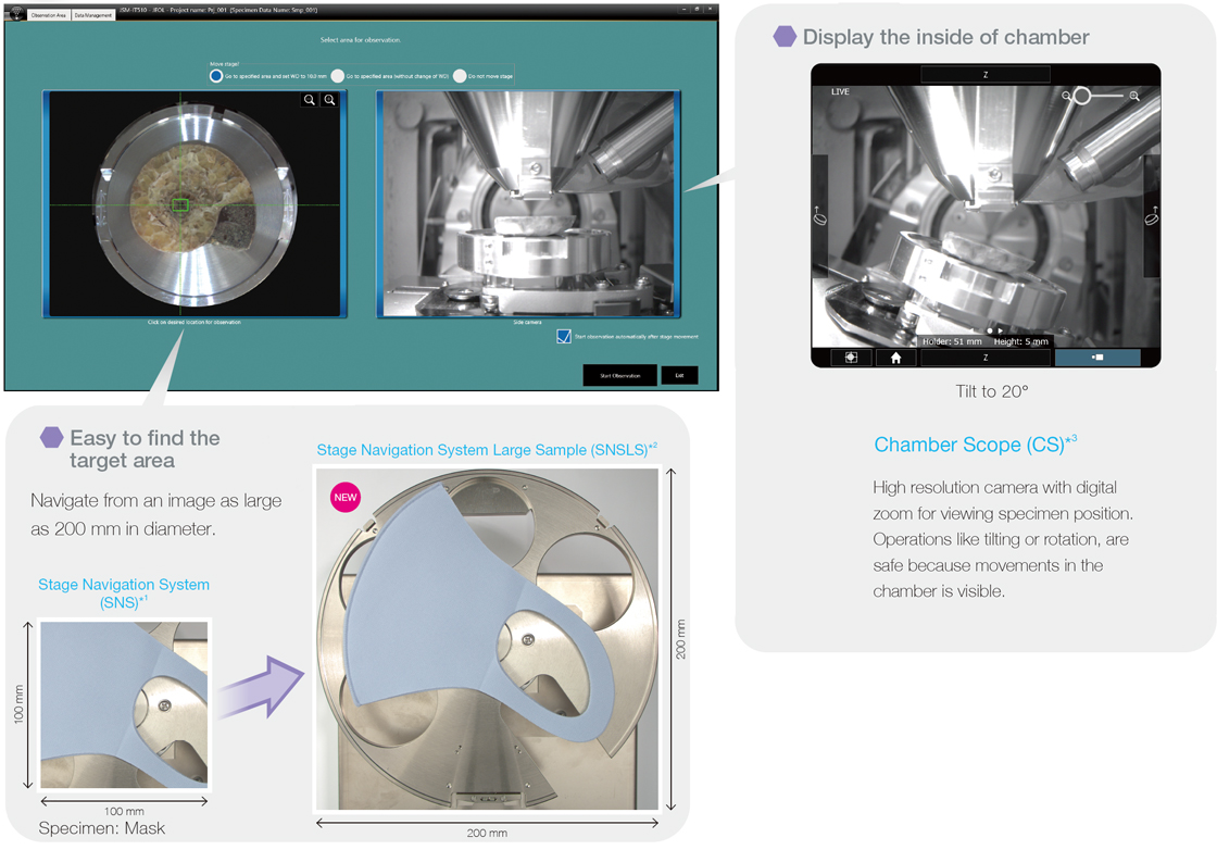
Stage Navigation System (SNS) is an option.
SNS Large Sample (SNSLS) is an option. Compatible with SNS.
Chamber Scope (CS) is an option.
3. Start observation automatically
Automatic image formation after evacuation.
Zeromag
Magnify the optical image *1, transition to SEM image
The Zeromag function simplifies navigation providing a seamless transition from the optical to SEM image.
The SEM, optical image and holder graphic are all linked for a global view of analysis locations.
Stage Navigation System (SNS) is needed to display the optical image.
Specimen: Fossil of ammonite
Accelerating voltage: 7 kV, Signal: BE
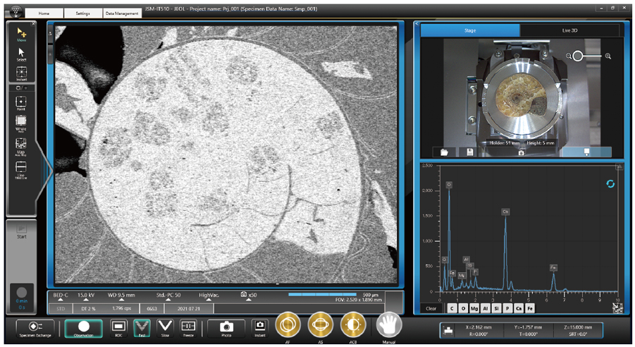
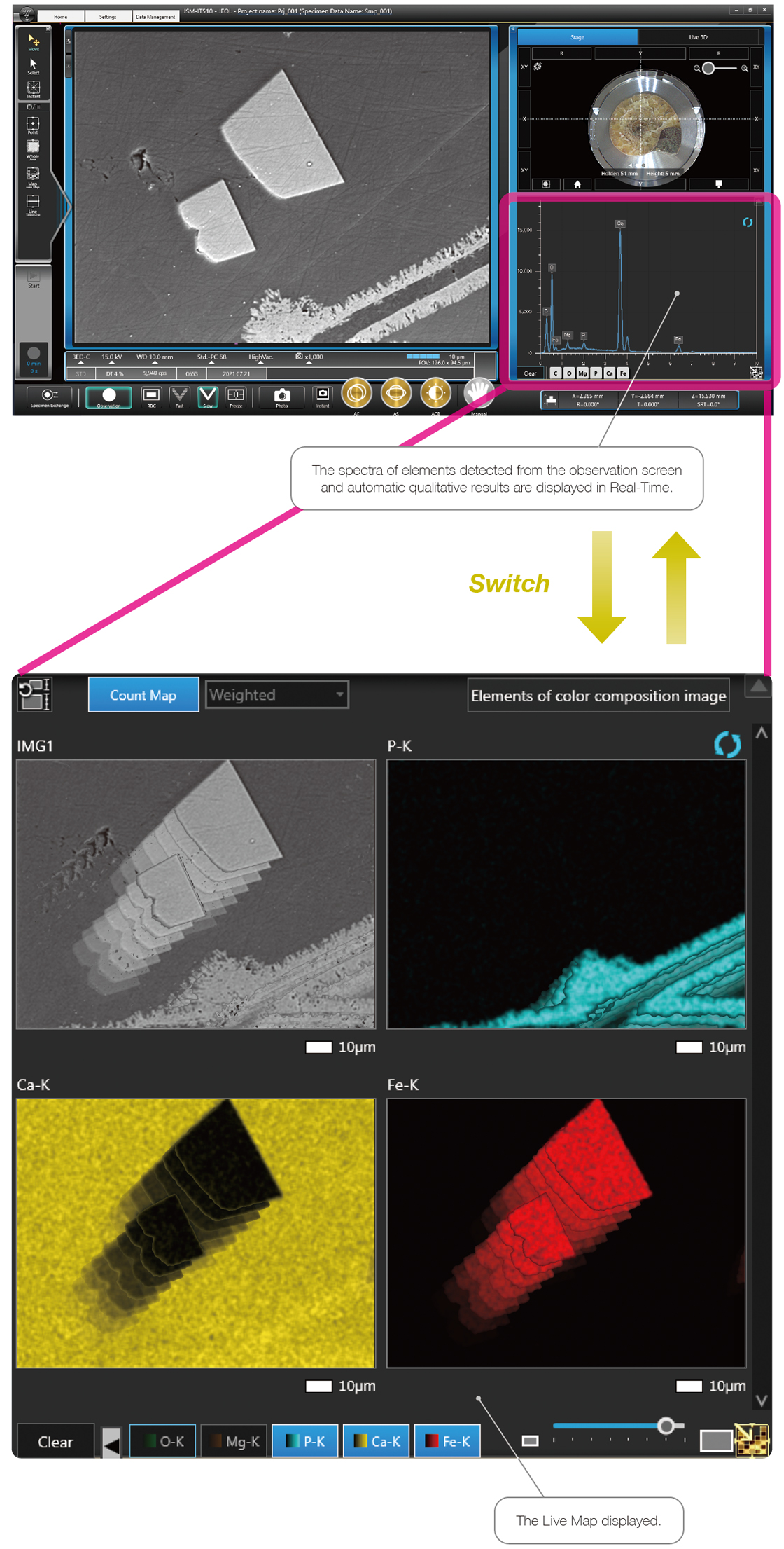
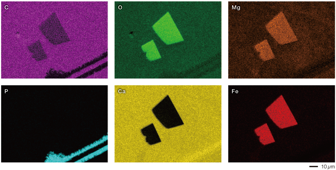
Live Analysis / Live Map*2
Embedded EDS for Real-Time elemental composition during observation
Live Analysis is a function which displays the EDS spectrum or element maps in Real-Time during image observation. This function can support searching and provide an alert for target elements.
Live Analysis is a standard for A (Analysis) / LA (Low Vacuum & Analysis).
Specimen: Fossil of ammonite
Accelerating voltage: 15 kV, Magnification: ×1,000
Simple analysis
The EDS analysis can be started within 3 clicks.
Video introducing the JSM-IT510
Functions of Live Map are introduced.
◆Clicking the Play button starts the video (approx. 2 minutes).
Variety of advanced options
Low-vacuum Hybrid Secondary Electron Detector (LHSED)*
This new detector collects both electron and photon signals providing an image with high S/N and enhanced topographic information.
LHSED is an option. And LV (Low Vacuum) or L A (Low Vacuum & Analysis) is also required.
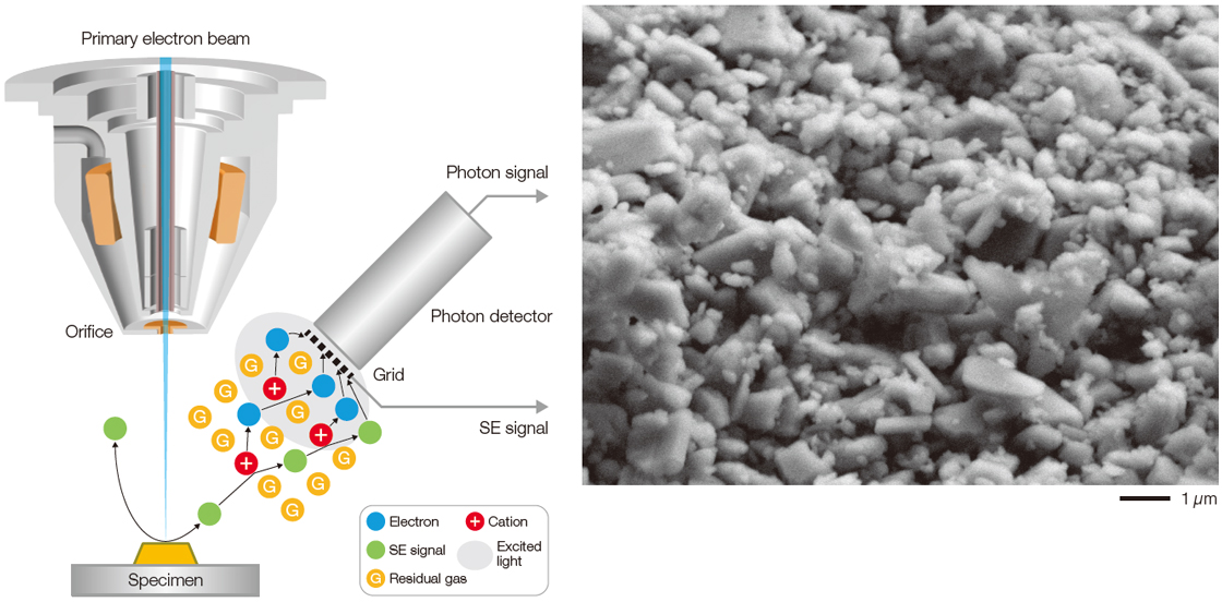
The mechanism of LHSED
Specimen: Plaster
Accelerating voltage: 7 kV, Magnification: x10,000, Signal: LV SE
Live 3D *
The images obtained by a new quadrant BE detector* can be displayed as a live 3D image.
3D images can clearly represent the shape of a specimen, even for those with subtle topographic information.
Live 3D is a standard in LV (Low Vacuum), LA (Low Vacuum & Analysis). BE detector (option) can be equipped on BU (Base Unit), A (Analysis).
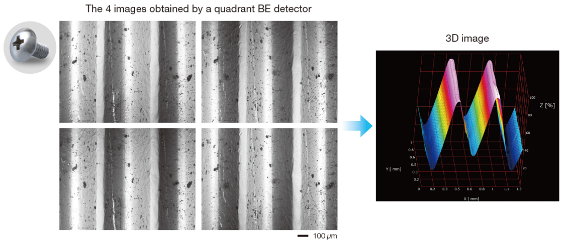
Specimen: Screw
Accelerating voltage: 15 kV Magnification: x100 Signal: BE
Montage
Montage function automates large area image collection and stitching of these images into a composite image.
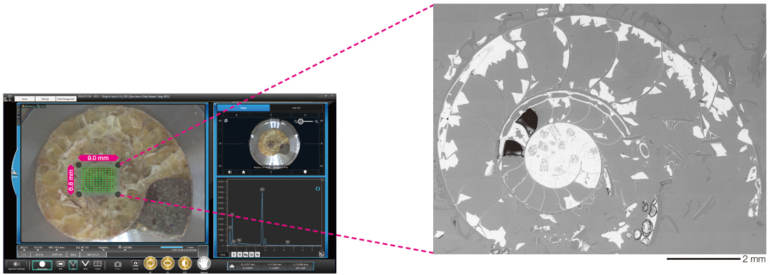
Specimen: Fossil of ammonite
Accelerating voltage: 15 kV, Magnification: x150, Signal: BE, Number of field: 13 x 13
Stage Navigation System (SNS) is needed to display the optical image.
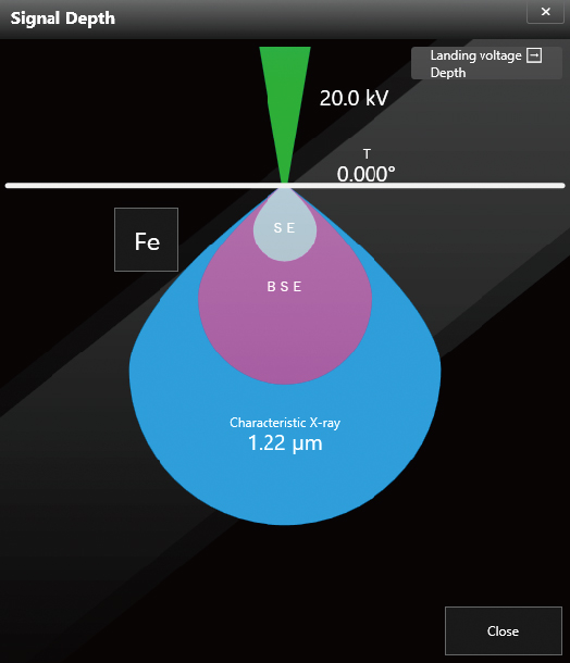
Display the depth of signal
This function displays the analysis depth (approx.) in the specimen.
For element analysis, it is very useful.
Link
News Release
Release of the New Scanning Electron Microscope JSM-IT510 Series InTouchScope™
Research Publications Using JSM-IT510
Specifications
Technical DATA
JSM-IT510 series can be equipped in the following 4 configurations: BU (Base Unit) / A (Analysis) / LV (Low Vacuum) / LA (Low Vacuum & Analysis).
| BU (Base Unit) | Basic type for observation under high vacuum |
|---|---|
| A (Analysis) | Analysis type, EDS is attached on BU as a standard |
| LV (Low Vacuum) | Low Vacuum type, for high and low vacuum operation. BED included. |
| LA (Low Vacuum & Analysis) | Low vacuum type, for high and low vacuum operation, BED and EDS included. |
SEM specifications
| Resolution | High vacuum mode 3.0 nm (30 kV), 15.0 nm (1.0 kV) Low vacuum mode※1 4.0 nm (30 kV BED) |
|---|---|
| Photo magnification | ×5 to ×300,000 (Defined with a photo size of 128 mm × 96 mm) |
| Display magnification | ×14 to ×839,724 (Defined with a photo size of 358 mm × 296 mm) |
| Electron gun | W filament, fully automatic gun alignment |
| Landing voltage | 0.3 kV to 30 kV |
| LV pressure adjustment※1 |
10 to 650 Pa |
| Objective lens aperture | Four stage, with XY fine adjustment function |
| Automatic function | Filament adjustment, Gun alignment adjustment Beam alignment Focus/ Astigmatism / Brightness / Contrast correction |
| Maximum specimen size |
200 mm diameter × 75 mm height 200 mm diameter × 80 mm height※3 32 mm diameter × 90 mm height※3 |
| Specimen stage | Large eucentric stage X:125 mm Y:100 mm Z:80 mm tilt: -10 to 90° rotation: 360° |
| Image mode | Secondary electron image, REF image, Compositional image* 1 Topographic image※1, Shadow image※1、PD image※4 |
| Image size | 640 × 480 1,280 × 960 2,560 × 1,920 5,120 × 3,840 |
| Photo assist function | Montage, Simple SEM, Zeromag, Live 3D |
| Operation support function |
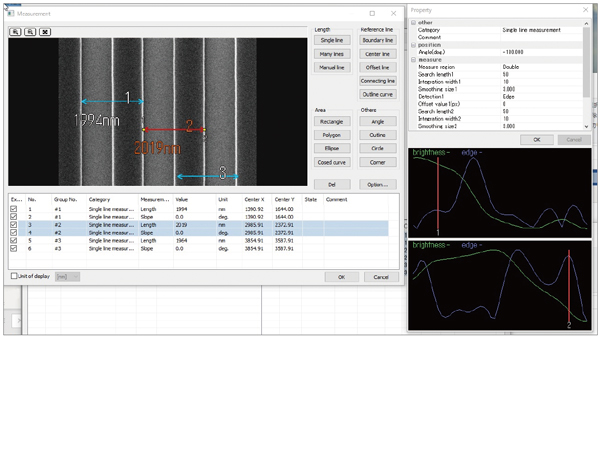
Recipe (Standard recipe / Custom recipe) Measurement (distance between 2 points, distance between parallel lines, angle, diameter etc.) Specimen exchange navi Signal depth function 3D measurement※5 |
| OS | Microsoft® Windows®10 64bit |
| Observation monitor | 23.8 inch touch panel |
| EDS functions※2 | Refer to EDS specification |
| Data management | SMILE VIEW™ Lab |
| Report generation One-click report |
Output to Microsoft®Word Output to Microsoft®PowerPoint※6 |
| Language switch | Japanese, English, Chinese※7 (operable on UI) |
| Vacuum system | Full automatic, TMP: 1, RP: 1 or 2※1 |
Main options
Backscattered Electron Detector (BED)*1
Low Vacuum Hybird Secondary Electron Detector (LHSED)
Low Vacuum Secondary Electron Detector (LVSED)
Energy Dispersive X-ray Spectrometer (EDS)*2
Wavelength Dispersive X-ray Spectrometer (WDS)
Electron Backscatter Diffraction Pattern (EBSD)
Load Lock Chamber (pre-evacuation chamber)
Stage Navigation System (SNS)
Stage Navigation System Large Sample (SNSLS)
Chamber Scope (CS)
Operation Panel (OP2)
LaB6Electron Gun (LAB6)
3D Analysis Software (SVM)
Table (TBL)
EDS specifications
Applicable to A (Analysis) / LA (Low Vacuum & Analysis)
●:Standard ○:Option
| Standard | ||
|---|---|---|
| Control PC | OS:Microsoft®Windows®10 64bit※8 | ● |
| Language | Japanese / English / Chinese※7 | ● |
| Detector | SDD type | Select from the detector list |
| Spectral analysis |
Qualitative analysis (peak identification, automatic qualitative analysis) Visual peak ID Standard-less quantitative analysis (ZAF method) Standard quantitative analysis (ZAF method)※9 PHI-RHO-Z (PRZ) method: quantitative correction method QBase (Qualitative analysis database) |
● |
| Line analysis | Line analysis (parallel & arbitrary direction) | ● |
| Elemental map |
Elemental map (map with multiple colors, monochrome, multiple-color superimposition) Maximum pixel resolution: 4,096 × 3,072 Real-time pop-up spectrum Deconvolution map (net count map, quantitative map) Real-time net count map Real-time filter Line profile display Probe tracking Playback analysis (time resolved spectral map) |
● |
| Serial analysis | Spectral analysis, Line analysis, Elemental map Comprehensive analysis of already-analyzed data (qualitative & quantitative analysis) |
● |
| Montage | Automatic montage (SEM image, Elemental map) Serial elemental mapping for multiple areas |
● |
| Particle analysis software |
・Particle analysis (auto / manual) & EDS analysis, Classification of particle analysis data, Graph display of statistical processed particle analysis data, Large-area serial particle analysis ・GSR (Gun Shot Residue) library ・Metal feature analysis library ・Automobile parts cleanliness analysis library |
○ ○ ○ ○ |
| Report generation | SMILE VIEW™ Lab Output as Microsoft®Word, Microsoft®PowerPoint file※6 |
● |
| SEM integration | Integrated management of observation & analysis data Specifying analysis position on the SEM operation screen (Direct analysis on UI for SEM) Graphical display of analysis positions |
● |
| Help function | Help guide | ● |
| Dual detector | Analysis with two detectors※10 | ○ |
| Off-line function | License software for off-line data analysis | ○ |
Standard in JSM-IT510LV / LA.
Standard in JSM-IT510A / LA.
An optional holder is required.
LHSED (option) is required.
SVM (option) is required.
Microsoft® Offce must be installed.
Chinese is optional.
For JSM-IT510A / LA, EDS software is installed on the same PC as SEM control software.
The optional probe current compensation unit (option) is required. Automatic monitoring of the probe current is possible only when EDS is connected to the microscope PC.
Two EDS detectors with the same active sensor size are required. There is a limitation for stage movements depending on installation ports.
Specifications subject to change without notice.
Microsoft, Windows, PowerPoint and Microsoft Office are registered trademarks of Microsoft Corporation in USA and other countries.
Microsoft Word is a product name of Microsoft Corporation.
Catalogue Download
JSM-IT510 InTouchScope™ Scanning Electron Microscope
Application
Application JSM-IT510
Gallery
Metal
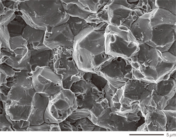
Crystalline observation of steel
For crystalline materials, such as metals, the contrast (channeling contrast) caused by the difference in crystal orientation can be imaged.
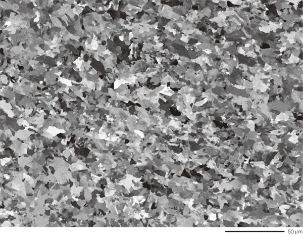
Specimen: Cross section of high-tension steel, Accelerating voltage: 5 kV,
Magnification: x500, Signal: BE
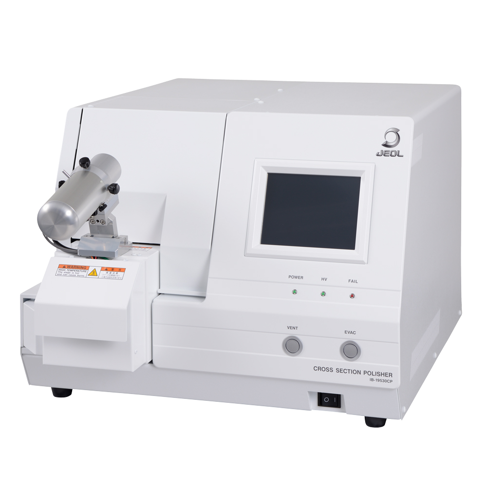
CROSS SECTION POLISHER™ IB-19530CP *1
CROSS SECTION POLISHER™ (CP) is designed for producing cross section or surface milling by using a broad Ar ion beam to irradiate the specimen.
Compared with mechanical milling, CP can easily produce a fine cross section without distortion.
Sold separately.
Fracture surface observation
Fracture surface observation by SEM is widely used to study the causes of failure and crack growth.
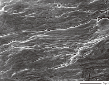
Striations produced by fatigue fracture
Specimen: Austenitic stainless steel, Accelerating voltage: 10 kV, Magnification: x5,000, Signal: SE
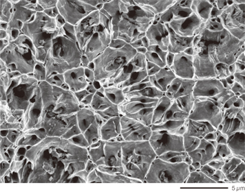
Dimples produced by ductile fracture
Specimen: Austenitic stainless steel, Accelerating voltage: 10 kV, Magnification: x5,000, Signal: SE
Rock candy pattern produced by intergranular fracture
Specimen: Austenitic stainless steel, Accelerating voltage: 10 kV, Magnification: x5,000, Signal: SE
Semiconductor
Resist pattern observation
In semiconductor fabrication, quality management of resist by SEM is very important.
The process can be confirmed by imaging the cross section of the resist pattern. Measuring line width is also possible.
Cross section of resist pattern (tilt to 35°)
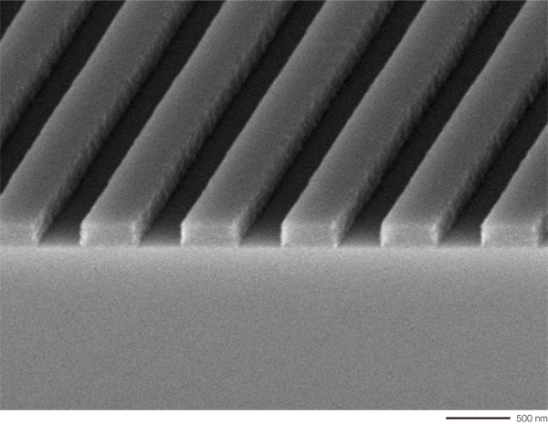
Accelerating voltage: 8 kV, Magnification: x30,000, Signal: SE
Resist pattern written on a Si wafer
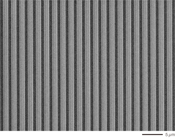
Accelerating voltage: 10 kV, Magnification: x3,000, Signal: SE
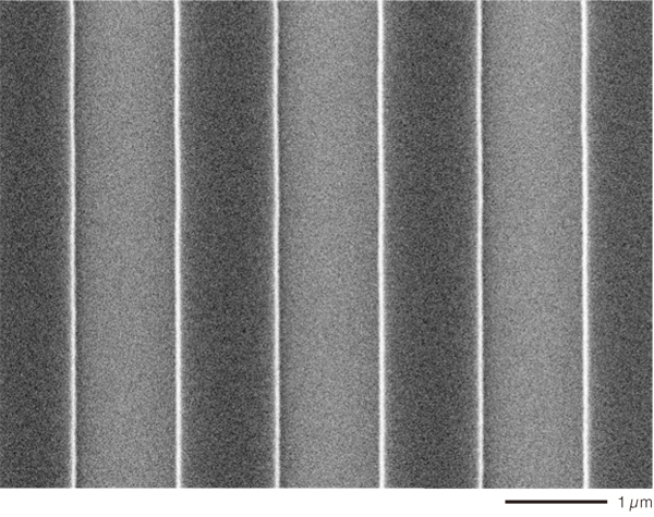
Accelerating voltage: 10 kV, Magnification: x20,000, Signal: SE
Printed circuit board (PCB) inspection
SEM is an effective instrument in quality management of PCB.
The low vacuum condition enables direct observation of the PCB without pre-treatment.
Chip condenser on the PCB
Accelerating voltage: 15 kV, Magnification: x45, Signal: Mixed signal
(LV backscattered electron: LV secondary electron = 3:7)
Image analysis software* allows measuring line width automatically.
Option. MultiImageTool (produced by SYSTEM IN FRONTIER INC.)
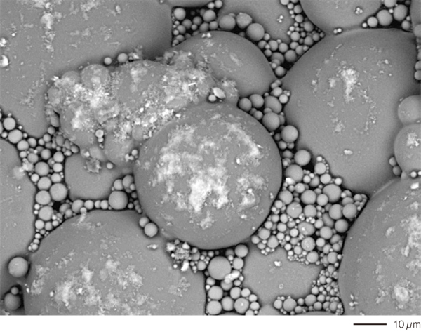
Soft material / Polymer
JSM-IT510 under low vacuum condition is suitable for direct observation of non-conductive specimens, such as superabsorbent polymer and mask.
Superabsorbent polymer
Accelerating voltage: 10 kV, Magnification: x1,000, Signal: LV SE
Non-woven mask
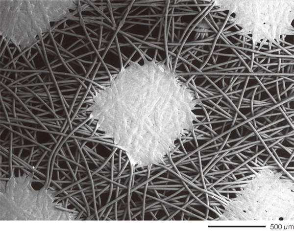
Accelerating voltage: 10 kV, Magnification: x50, Signal: LV BE
Accelerating voltage: 10 kV, Magnification: x1,000, Signal: LV BE
Urethane mask
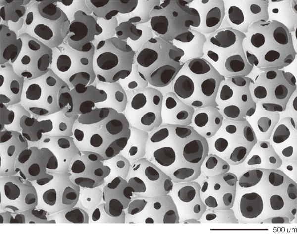
Accelerating voltage: 10 kV, Magnification: x50, Signal: LV BE
It is possible to obtain SE image and BE image simultaneously.
The SE image provides shape information.
The BE image shows bright areas indicating higher atomic number composition for this area.
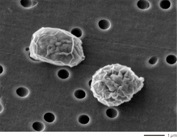
Biology
The normal shape of biological specimen, such as cells or microorganisms, can be confirmed after pre-treating them by chemical fixation or freeze drying method to keep their shape.
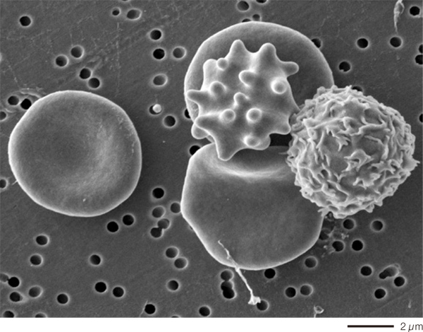
Erythrocyte and leukocyte
Accelerating voltage: 3 kV, Magnification: x7,000, Signal: SE
Chlorella
Accelerating voltage: 3 kV, Magnification: x15,000, Signal: SE
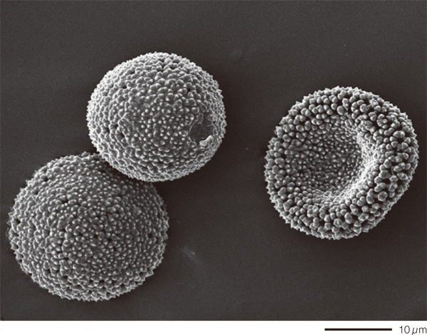
Daphne pollen
Accelerating voltage: 10 kV, Magnification: x2,000, Signal: SE
More Info
Are you a medical professional or personnel engaged in medical care?
No
Please be reminded that these pages are not intended to provide the general public with information about the products.