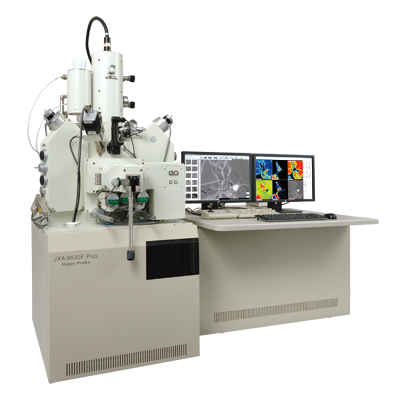
【DISCONTINUED】JXA-8530FPlus Field Emission Electron Probe Microanalyzer
DISCONTINUED
This product is no longer available.
If you would like to know the latest information about your preferred product or to find out more about alternatives, please click on the link below. We hope you will continue to use our products.
JEOL commercialized the world's first FE-EPMA, the JXA-8500F in 2003. This highly regarded FE-EPMA has long been used in various fields, such as: metals, materials and geology in both industry and academia. The JXA-8530FPlus is a third-generation FE-EPMA that comes with enhanced analytical and imaging capabilities. The In-Lens Schottky field emission electron gun combined with new software provides higher throughput while maintaining high stability, thus allowing a wider range of EPMA applications to be achieved with higher resolution.
Features
In-Lens Schottky Plus FEG EPMA version
The In-Lens Schottky Plus FEG EPMA version, with an optimized angular current density, allows for analysis with a large probe current of 2μA or more. The resolution of secondary electron image has been improved even under analytical conditions by automatically adjusting for the correct convergence angle.
Advanced software
A wealth of Microsoft Windows®-based advanced applications systems are available, including:
Trace Element Analysis Program for simpler, optimized analysis of trace elements including adding data collected from up to 5 spectrometers,
Phase Map Maker for automatic creation of phase maps based on principal components,
Non-Flat Surface Analysis Program for automated WDS analysis of specimens with surface irregularities. This is possible due to the large Z travel of the stage (7.5 mm).
Notices:Windows is a registered trademark of Microsoft Corporation in the United States and other countries.
Flexible WDS configuration
Various X-ray spectrometers (WDSs) can be selected: a Rowland circle radius of 140 mm (140R) or 100 mm (100R), 2 crystal or 4 crystal configurations and a mix of standard or large size crystals.
The XCE (2 xtl) X-ray Spectrometer, the FCS (4 xtl) X-ray spectrometer and the L (large 2 xtl) X-ray Spectrometer for 140R have wide spectrometry range and provide superior wavelength resolution and peak-to-background ratio. The H Type X-ray Spectrometer of 100R provides high X-ray intensity. Users can select from these spectrometers depending on requirements.
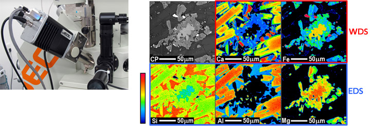
Combined WDS/EDS system
The JXA-8530FPlus comes with JEOL's 30mm2 silicon-drift detector (SDD).
A high count-rate SDD along with an in-situ variable aperture enables EDS analysis at WDS conditions. EDS spectra, maps and line scans can be acquired simultaneously with WDS data.
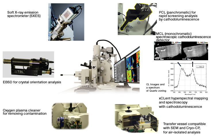
Multipurpose chamber
The JXA-8530FPlus is equipped with a highly-expandable specimen chamber and specimen exchange chamber, enabling you to integrate a variety of optional attachments on the chamber.
These include:
Electron Backscatter Diffraction System (EBSD)
Tilting rotating sub-stage
Cathodoluminescence Detectors (panchromatic, monochromatic, full color hyperspectral)
Soft X-ray Emission Spectrometer
Air Isolated Transfer Vessel
High Etching Rate Ion Source, in-situ cleaner, etc.
Powerful clean vacuum system
A powerful, clean vacuum system is employed on the JXA-8530FPlus, including two magnetic-levitation turbo molecular pumps. In addition, a two-stage intermediate chamber is provided for the electron optical column, thus maintaining high vacuum in the electron-gun chamber by differential pumping.
The addition of optional Scroll pumps and a liquid nitrogen cold finger create the ultimate oil free vacuum system.
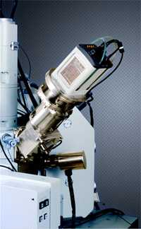
Soft X-ray Emission Spectrometer (SXES)
Soft X-ray Emission Spectrometer(SXES)
An ultra-high energy-resolution Soft X-ray Emission Spectrometer was co-developed by the Institute of Multidisciplinary Research for Advanced Materials, Tohoku University (Prof. M. Terauchi) and JEOL Ltd., etc.
The variable-line-spacing (VLS) grating enables simultaneous detection (much like EDS) and allows detection of Li-K and B-K spectra with a high-sensitivity CCD. This spectrometer achieves superbly high energy-resolution, enabling detailed chemical-bonding state analysis.
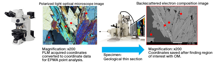
miXcroscopy (Correlative microscope)
miXcroscopy Linked Optical & Scanning Electron Microscopy System
Regions of interest, along with X-Y stage coordinates, located in the optical microscope can be recorded and transferred to the EPMA for navigation to the desired location for imaging and analysis.
Specifications
| Elemental analysis range | WDS: (Be) B to U, EDS: B to U |
|---|---|
| X-ray spectrometry range | WDS spectrometry range: 0.087 to 9.3 nm
EDS energy range: 20 keV |
| Number of X-ray spectrometers | WDS: 1 to 5 selectable, EDS: 1 |
| Maximum specimen size | 100 mm × 100 mm × 50 mm (H) |
| Accelerating voltage | 1 to 30 kV (0.1 kV step) |
| Probe current stability | ± 0.3%/h |
| Secondary electron image resolution | 3 nm at WD 11 mm, 30 kV |
| 20 nm at 10 kV, 10 nA, WD 11 mm
50 nm at 10 kV, 100 nA, WD 11 mm |
|
| Magnification | x40 to x300,000 (WD 11mm) |
| Scanning image pixel resolution | Up to 5,120 x 3,840 |
Catalogue Download
JXA-8530FPlus Field Emission Electron Probe Microanalyzer
Application
Application JXA-8530FPlus
More Info
Are you a medical professional or personnel engaged in medical care?
No
Please be reminded that these pages are not intended to provide the general public with information about the products.