electron backscatter diffraction, EBSD
electron backscatter diffraction
A method to measure the local orientations of a crystalline specimen from an electron backscatter diffraction pattern (EBSD or EBSP), where a bulk specimen is largely tilted (about 70°) from the horizontal plane and is probed by the electron beam to acquire an EBSD pattern as shown in Fig. 1.
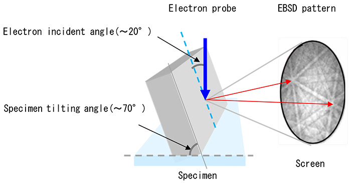
Fig. 1 Schematic of EBSD pattern acquisition
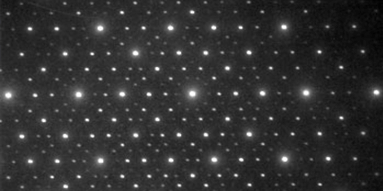
Fig. 2 shows schematically the formation of the EBSD pattern. The electrons incident onto the specimen (i) are elastically or inelastically scattered over a large angular range (ii) by the constituent atoms of the specimen. Among these electrons, the electrons travelling in a direction θ satisfying the Bragg condition (2d・sinθ=n・λ) with respect to the crystal lattice plane (iii) are diffracted and produce diffraction spots on the screen. Here, d is the spacing of the lattice plane, θ is the angle between the electron beam and the lattice plane, n is the positive integer and λ is the electron wavelength. The electrons travelling in different azimuthal directions φ with maintaining the Bragg condition (conical electron beams (iv)) also produce successive diffraction spots, forming a diffraction line (v). Many diffraction lines generated from the many lattice planes in different orientations are superposed and thus form an EBSD pattern. (This pattern is the same as the Kikuchi pattern already well known.) Fig. 3(a) and (b) show EBSD patterns obtained respectively from alumina (Al2O3) and from copper (Cu).
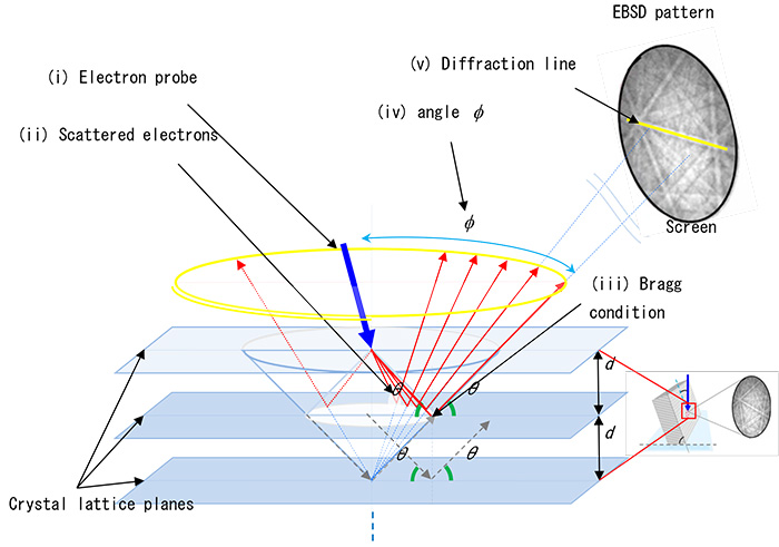
Fig. 2 Schematic of formation of EBSD pattern
The electrons which travel in the direction θ satisfying a Bragg condition (2d・sinθ=n・λ) with respect to the crystal lattice planes (lattice spacing: d) and in different azimuthal directions φ(conical electron beams), form a diffraction line. Superposition of many diffraction lines generated from many lattice planes with different orientations produces an EBSD pattern.
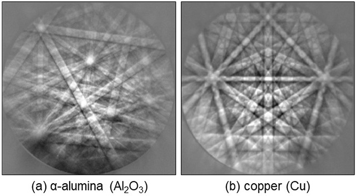
Fig. 3 EBSD patterns (a) α-alumina (Al2O3) (b) Copper (Cu)
Elastically and Inelastically scattered electrons closer to the incident electron beam direction have stronger intensity. Thus, for a larger specimen tilt angle with respect to the horizontal plane (for a small electron incident angle to the specimen), a higher intensity EBSD pattern is obtained. When the specimen tilt angle becomes small and the electron incident angle reaches 40° or more, the intensity of the EBSD pattern rapidly decreases. Thus, the EBSD pattern is acquired usually at a specimen tilt angle of about 70° to the horizontal plane or at an incident electron probe angle of approximately 20°.
The EBSD pattern is projected on a screen, which is placed against the tilted specimen and makes an angle of about 90° with respect to the optical axis of the electron beam. The projected EBSD pattern is stored in a PC using a CCD camera or a CMOS camera. Then, the EBSD pattern is compared with the simulated patterns computed based on the structure of the specimen. As a result, the crystal orientation at the electron-probe irradiation point is determined. Since the EBSD method assumes that the crystal structure of the specimen is known, the method cannot be applied to the specimen with an unknown crystal structure.
The smallest area (spatial resolution) of the crystal orientation measurement is approximately 0.2 μm in diameter for a thermionic-emission SEM equipped with a tungsten (W) filament and 10 to 20 nm in diameter for a high-resolution SEM equipped with a Schottky-emission electron gun. These values are almost equal to the electron-probe diameter when the probe current is approximately 1 nA. The specimen depth to generate the EBSD pattern ranges down to 30 to 50 nm from the specimen surface, though it depends on the accelerating voltage and the atomic numbers of the constituent elements in the specimen. The electrons scattered into deeper than this range suffer energy losses many time due to inelastic scattering, creating electrons with various wavelengths. Then, these electrons do not form the EBSD pattern.
An important feature of the EBSD method is crystal orientation mapping. That is, when the electron probe scans an arbitrary area of the specimen, the crystal orientations of each measurement point of the area are displayed and a crystal orientation map can be obtained automatically and rapidly. The speed of sequential measurement is approximately 60 to 3,000 points per second, though it depends on the image quality of the EBSD pattern and the image acquisition conditions.
Makers of developing EBSD systems provide a wealth of application software programs, which display a variety of information on the orientations of the crystalline specimen. Main application software programs include: 1) a program displaying a color map of the crystal orientations using color keys against the inverse pole figure (IPF). 2) a program displaying the grain boundaries. 3) a program displaying the crystal quality of each crystalline grain with a gray scale utilizing the difference in the sharpness of the EBSD pattern at each measurement point.
Fig. 4 shows an example of EBSD analysis applied to a neodymium magnet (Nd2Fe14B). Fig. 4(a) is a secondary electron image of a specimen position subjected to EBSD analysis. Fig. 4(b) is a crystal orientation map (also termed to be an inverse pole figure (IPF) map), which displays the orientations of the crystalline grains in the specimen using color keys in the figure to the right of (b). The orientations of the lattice planes vertical to the specimen surface are shown. Fig. 4(c) is an image showing crystalline grain boundaries with dark lines. This image is formed by intensity difference between successive measurement points (differential image). Since the crystal orientations are the same in the grains, the bodies of the grains are shown bright. Fig. 4(d) is an Image Quality (IQ) map displaying the quality of crystallinity. Bright crystal grains indicate to have high crystal quality (sharp EBSD patterns). Less bright grains indicate to have low crystal quality (smear EBSD patterns).
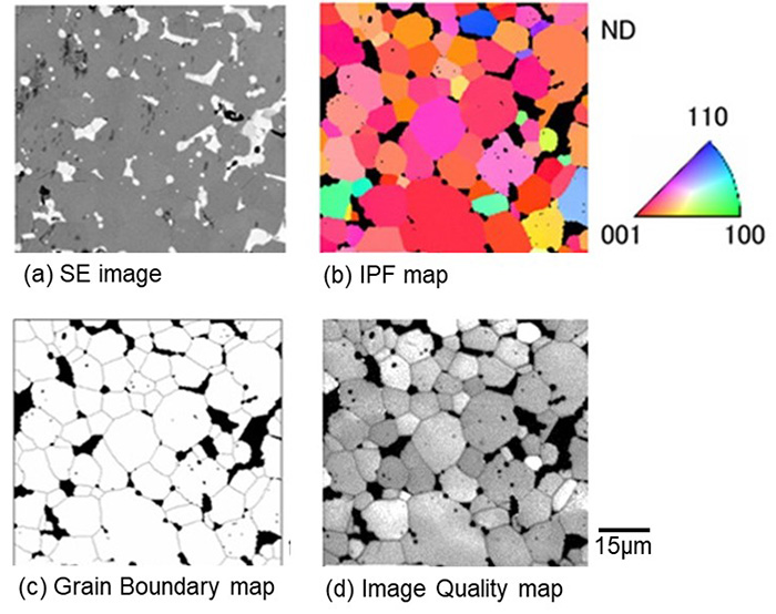
Fig. 4 EBSD analysis of a neodymium magnet (Nd2Fe14B).
- Secondary electron image.
- Crystal orientation (IPF: inverse pole figure) color map of the crystal grains in the specimen. Color keys for the IFP (the right of (b)) are used for the color presentation.
- Grain boundary map. The specimen positions at which the crystal orientation difference from the adjacent measurement points is larger than a certain angle, are displayed as dark (differential image map). Then, the crystalline grain boundaries are elucidated as dark lines. It is noted that the dark-color areas are regarded as amorphous regions.
- Image Quality (IQ) map. The crystal quality of the grains is displayed with a gray scale. The grains with a high crystal quality is shown bright and the grains with a low crystal quality is shown dark utilizing image sharpness of the acquired EBSD pattern. Black-color areas indicate the regions where EBSD patterns were not observed.
Data courtesy: The application example of EBSD analysis of a neodymium magnet (Nd2Fe14B) is supplied by the JFE Techno-Research Corporation
Related Term(s)
Term(s) with "electron backscatter diffraction" in the description
Are you a medical professional or personnel engaged in medical care?
No
Please be reminded that these pages are not intended to provide the general public with information about the products.