backscattered electron detector, BE detector, BSE detector
backscattered electron detector, BE detector, BSE detector
The most widely used backscattered electron (BE) detector is a silicon (Si) semiconductor detector. The detector enables us to obtain the compositional image and the topographic image of a specimen. (Some JEOL SEMs display the compositional image as BED-C and the topographic image as BED-T on the monitor screen.
The BE detector is usually made of an annular-shaped thin plate and called the annular BE detector. The detector is placed just below the objective lens. The incident electrons pass through the center hole of the detector (Fig. 1). Since the backscattered electrons have high energies, they travel straight and come to the detector. Thus, it is not necessary to apply a voltage to the detector for collecting the electrons, unlike the case of secondary electrons.
As the BE detector is thin, it does not interfere insertion of an energy-dispersive X-ray spectroscopy (EDS) detector for elemental analysis into the microscope column, enabling observation of the compositional and topographic images and analysis of the constituent elements simultaneously. Not only a secondary electron detector (ET detector) but also the other optional detectors, a wavelength-dispersive X-ray spectrometer (WDS) and/or a soft X-ray emission spectrometer (SXES), can also be installed together with the BE detector and operated simultaneously. For high-magnification observation, the specimen is needed to bring close to the objective lens and the working distance (WD) must be less than 3 mm resulting in overlap of the specimen and the detector. Thus, the BE detector is often constructed to be temporarily retractable from the microscope column.
The Si semiconductor annular BE detectors include two-segmented type, four-segmented type and more-segmented type. Among them, the four-segmented detector is mainly used. For convenience, Fig. 1 illustrates a two-segmented detector as an example. In a two-segmented detector (A and B in Fig. 1), the compositional image can be obtained by adding the output signals from the two segments, and the topographic image can be obtained by taking difference between the two signals.
There are SEM instruments equipped with the second semiconductor detector to detect the electrons backscattered at low angles viewed from the specimen (C in Fig. 1), in addition to the above-mentioned annular BE detector. If the electrons backscattered only at low angles are detected by this second detector, the shadowing effect, an effect of illuminating specimen from an oblique direction, is enhanced or the shaded area becomes larger (longer), resulting in an image with a more three-dimensional effect. (Some JEOL SEMs display the shadow image as BED-S on the monitor screen.
High-resolution SEMs, in some cases, employ an additional detector placed inside the microscope column (D in Fig. 1). This detector allows to detect only the electrons backscattered at high angles near the direction of the incident electrons, making it possible to acquire only the compositional image without topographic nature.
If a high-speed response for backscattered electron signals is needed, a high-response-speed detector like an yttrium aluminum garnet (YAG) scintillator detector can be used instead of the BE detector. It is however noted that the scintillator detector is difficult to form segment-shaped, and thus not possible to emphasize or erase the topographic image, which can be performed by the BE detector.
Principle of the Si semiconductor detector
The principle of the semiconductor detector is as follows (illustrated in Fig. 2). The detector uses a PN-type photodiode, which consists of a junction of a “P” layer and an “N” layer of Si. The “depletion layer”, where conduction electrons and holes do not exist, is formed at the junction of the P layer and the N layer. When backscattered electrons enter the detector, electron-hole pairs are created in the depletion layer. Then, the potential difference between the P layer and the N layer causes the electrons to flow to the N layer and the holes to the P layer. The electric current due to the flow of those electrons and holes is amplified and used to form a backscattered electron image.
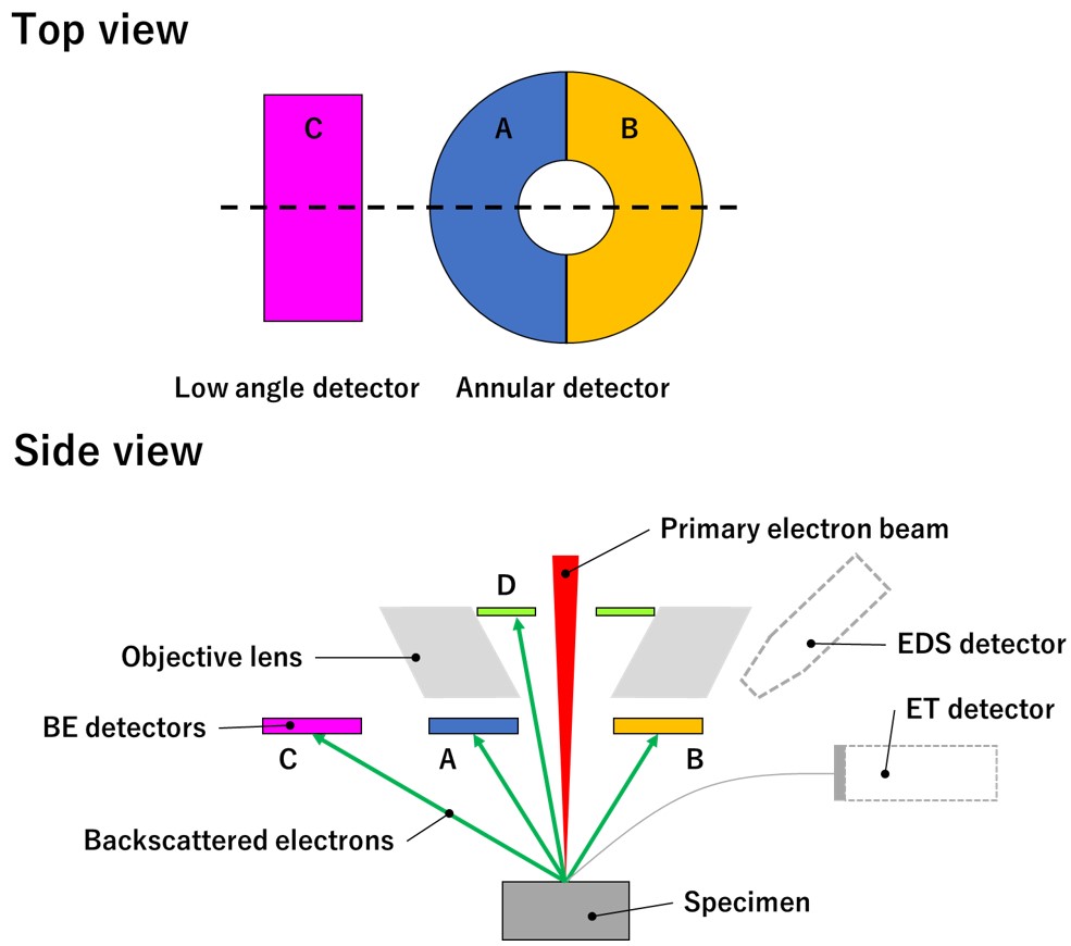
Fig. 1. Schematics of arrangements of the Si semiconductor BE detectors.
The annular BE detector (pair of A and B), the low-angle detector C, and the in-column BE detector D. The upper figure is the top view of the detectors. The lower figure shows the side view of the arrangement of the detectors along the dotted line in the upper figure relative to the objective lens, the specimen, the SE (secondary electron) detector and the EDS detector (including the incident electron path and the backscattered electron path).
The backscattered electrons increase towards the direction perpendicular to the specimen surface. When the specimen surface is uneven, the backscattered electron intensities detected by the detectors A and B are different. If the signals from A and B are added (A+B), the compositional image is obtained with erasing the topographic image. If the signal B is subtracted from signal A, (A–B), the topographic image is obtained with an emphasis. When the electrons backscattered at low angles detected by the detector C are added to the compositional image (A+B+C), a strong shadowing effect arises, that is the shaded area becomes long, or a three-dimensional effect is enhanced.
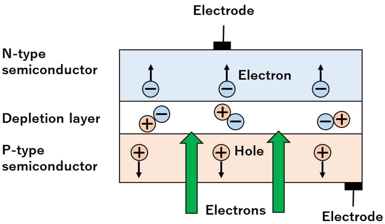
Fig. 2. Conceptual diagram of the action of the PN-type photodiode when electrons are incident on it.
Related Term(s)
Term(s) with "backscattered electron detector, BE detector, BSE detector" in the description
Are you a medical professional or personnel engaged in medical care?
No
Please be reminded that these pages are not intended to provide the general public with information about the products.