cathodoluminescence
cathodoluminescence
Electrons in a solid are excited by electron-beam irradiation leaving holes. The electrons recombine with the holes to emit light (ultraviolet to infrared). This phenomenon is called "Cathodoluminescence". Cathodoluminescence is utilized as a method to analyze the electronic structure of solids in an electron microscope. The method can measure local electronic states (energy levels) of impurities and defects, the electronic states being formed between the valence band and the conduction band (in the forbidden band). Thus, the method enables the evaluation of inorganic materials containing the structural defects with a high spatial resolution (better than 1 μm) by the combined use with structural information obtained from SEM / STEM / TEM images. Applications to biological specimens, such as detection of specific proteins, have also been studied.
- In the case of semiconductors, electrons in the valence band are excited to the conduction band by incident electrons with generating holes in the valence band (referred to as electron-hole pair generation). The excited electrons and holes form a pair (free exciton (FX): It occurs remarkably at low temperatures) bound by Coulomb force. Free excitons are unstable and recombine at arbitrary places and emit light. At room temperature or higher temperatures, the free excitons cannot be formed, thus the generated electrons and holes diffuse independently in the semiconductor as carriers. When they are trapped by impurity atoms creating donors and acceptors, radiative recombination occurs. When they are captured by lattice defects such as dislocations, non-radiative recombination occurs. For example, the distribution of impurity atoms can be detected from a CL image using a specific wavelength.
CL measurements of semiconductors have to be conducted at liquid nitrogen temperature or lower because the luminescence intensity weakens due to the increases of non-radiative recombination through the lattice vibrations. Also, the CL measurements have to be performed with an accelerating voltage less than 100 kV. : When the accelerating voltage of the incident electron beam exceeds the threshold voltage (approx. 100 kV), the generation of point defects increases. The point defects create deep defect levels within the forbidden band and non-radiative recombinations via those levels increase, causing decrease of the luminescence intensity. - In the case of insulators, impurity centers are formed by d-electrons of transition elements and f-electrons of rare earth elements when they are added in oxides or sulfides, and color centers are formed at vacancies in alkali halide crystals. These electrons trapped at such localized centers produce a ground level and an excited level within the forbidden band. Light emission occurs at the electronic transition between those levels, enabling positional information on additive elements to be obtained. Restriction on the accelerating voltage of the incident electron beam is not severe.
- In the case of organic materials, light is emitted by electronic transition from the lowest unoccupied molecular orbital (LUMO) of the organic molecule to the highest occupied molecular orbital (HOMO). Local information cannot be obtained, but information on degradation and aging of organic molecules can be obtained. Since the organic specimen is susceptible to electron-beam irradiation, observation at a low accelerating voltage is required.
(By Dr. Naoki Yamamoto, Tokyo Institute of Technology)
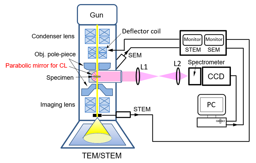
Fig.1 Schematic diagram of cathodoluminescence (CL) detection system.
Light emitted from a specimen in a STEM (SEM) by an incident electron beam is collected and reflected by a parabolic mirror, and becomes parallel light, then guided outside the electron microscope. This light passes through the lens 1 (L1) and is focused by the lens 2 (L2) onto the slit of the spectrometer in front of the CCD detector. The spectrum of the light passing through the slit is recorded with the CCD. The incident electron beam is two-dimensionally scanned using the beam deflector controlled with a computer, and the emission spectra from each beam position are successively acquired by the CCD. After measurement, a two-dimensional monochromatic CL image is displayed by selecting a specific wavelength. From the STEM or SEM image and the CL image of the specimen, the optical properties of the structural defects are obtained.
The luminescence ranges from infrared light (1 to 2.5 μm in wavelength) to ultraviolet light (200 nm to 380 nm). Specific gratings and detectors are used for ultraviolet-, visible- and infrared-light depending on the wavelength range. The wavelength resolution of the detector is approximately 1 nm (less than 10 meV in energy).
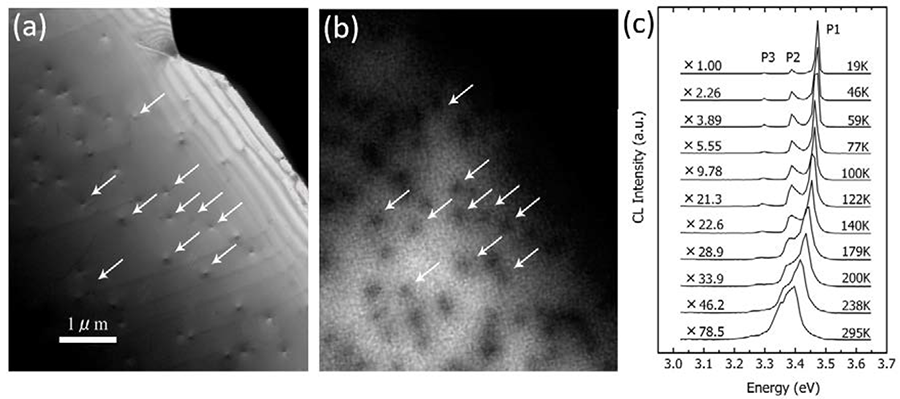
Fig.2 TEM dark field image, CL image and CL spectra of GaN epitaxial film containing the dislocations penetrating the specimen (accelerating voltage 80 kV)
A GaN epitaxial film grown by the MOCVD (metal organic chemical vapor deposition) method on a sapphire substrate (film thickness 4 μm) was thinned from the substrate side by ion milling. A transmission electron microscope (TEM) image and a CL image and CL spectra of a thin edge region containing the dislocations penetrating the specimen are shown.
(a) TEM dark field image. Arrows in the image indicate the dislocations.
(b) Monochromatic CL image of the same area in (a) taken at room temperature using an emission light with wavelength of 336 nm (3.39 eV).
It is seen that free exciton (FX) emission occurs in the whole area of the specimen (bright part). Dark contrast appears at the dislocations because the carriers are captured there and non-radiative recombination occurs.
(c) CL spectra measured at different specimen temperatures. The main peak (P1) is FX emission of GaN, the P2 peak is light emission associated with impurities, and the P3 peak is donor-acceptor pair emission (D, A). The FX emission intensity, which is important for elucidating the dislocation positions, decreases with increasing temperature, i.e., the intensity at room temperature is two orders of magnitude smaller than that at 19K. Thus, measurement at low temperature is necessary, especially for a thin specimen with a low emission intensity. From the analysis of the CL intensity distribution around a dislocation, the diffusion length of the carrier can be measured.
Related Term(s)
Term(s) with "cathodoluminescence" in the description
Are you a medical professional or personnel engaged in medical care?
No
Please be reminded that these pages are not intended to provide the general public with information about the products.