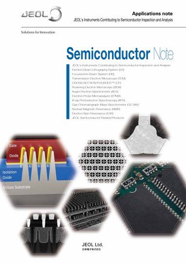
Semiconductor Note
What are Semiconductors?
Semiconductors are materials whose electrical conductivity lies between that of conductors (which readily allow the flow of electricity) and insulators (which resist the flow of electricity). Integrated circuits composed of numerous transistors and diodes, fabricated from semiconductor materials, are commonly referred to as semiconductors or semiconductor chips. Semiconductors are widely utilized in a broad range of applications, from home appliances and automobiles to critical social infrastructure.
Analytical Techniques in the Field of Semiconductors
Within the field of semiconductors, new materials such as SiC and GaN, advanced transistor structures, and cutting-edge 3D packaging technologies are receiving a significant attention for achieving lower power consumption and higher performance. To ensure high manufacturing yield and device reliability, precise characterization techniques and the appropriate selection of preprocessing and analytical instruments are essential. This semiconductor note introduces various analytical instruments and application examples, highlighting their use in semiconductor manufacturing and research.
JEOL's Instruments Contributing to Semiconductor Inspection and Analysis
-
Electron Beam Lithography System (EB)
- Application example using EB lithography system
- Column: The role and importance of EB lithography systems
- Focused Ion Beam System (FIB)
-
Transmission Electron Microscope (TEM)
- Application of TEM-Based CD Measurement in Advanced Semiconductor Processes
- 3-1 Creating a TEM Specimen of a FinFET
- 3-2 Structural and Compositional Analysis of FinFET
- 3-3 3D Construction of SiC Semiconductor Device
- 3-4 Plan-View TEM for Structural and Elemental Analysis of FinFET
- CROSS SECTION POLISHER™ (CP)
-
Scanning Electron Microscope (SEM)
- 5-1 Automatic Length Measurement of the EB Exposure Resist Pattern
- 5-2 Voltage Contrast Observation of the Semiconductor Chip After SRAM delayering
- 5-3 Simultaneous Cross-sectional Observation of Various Signals from the SiC Power Semiconductor
- 5-4 Stress Measurement for the Cross Section of SiC Power Semiconductor Diode
- 5-5 Lattice Defect Analysis of GaN wafer
- 5-6 Cross Section Preparation by CP and its Observation by SEM of the Junction Between the Au Bonding Wire and Semiconductor Chip
- 5-7 High Resolution Elemental Map of an IC Cross Section by Windowless EDS
-
Auger Electron Spectrometer (AES)
- 6-1 Visualization of Elements and Distribution by Chemical State in Semiconductor Multi-Chip CP Cross Sections
- 6-2 Measurement of the Band Gap in the SiO2 Film that has Formed on Top of the Si Substrate
- 6-3 Internal Potential Difference Analysis on the P-N junction in the SiC Power Semiconductor Diode
- 6-4 Analysis of Carbon-Derived Contamination in SiC
-
Electron Probe Microanalyzer (EPMA)
- 7-1 Analysis of Trace Elements in the Interface of a Solder Connection
- 7-2 High-Wavelength Resolution Analysis of Semiconductor Memory (SRAM)
-
X-ray Photoelectron Spectrometer (XPS)
- 8-1 Analysis of Organic Contamination on the Surface of Boards and Electronic Components
- 8-2 Analysis of Plating Corrosion on IC Chip Terminals
- 8-3 Analysis of Oxide Film Thickness on Solder Surfaces
-
Gas Chromatograph-Mass Spectrometer (GC-MS)
- 9-1 Automatic Structural Analysis of Unknown Compounds by AI for Semiconductor Analysis
- 9-2 Analysis of Impurities in Cleaning Solvent for Semiconductors
-
Nuclear Magnetic Resonance (NMR)
- 10-1 Composition and Impurity Analysis of Photoresists by NMR
-
Electron Spin Resonance (ESR)
- 11-1 Dangling Bond Measurement Using ESR
JEOL Semiconductor-Related Products
INDEX
Solutions by field
Are you a medical professional or personnel engaged in medical care?
No
Please be reminded that these pages are not intended to provide the general public with information about the products.