Not just secondary electrons! A new low-vacuum hybrid secondary electron detector that also detects light emission information (CL)
MP2025-02
Introduction
The low vacuum hybrid secondary electron detectors are now able to form secondary electron image from light signals, greatly improving the live image quality of the low vacuum secondary electron image. In addition, by switching modes, an image coming from a light emission signal (cathodoluminescence :CL) of a specimen due to electron-beam irradiation can be obtained. Accordingly, contrasts from crystal defects and impurities of very small quantity can be obtained, enabling observation and analysis that were not possible before.
Low vacuum hybrid secondary electron detector (LHSED)
The low vacuum hybrid secondary electron detectors are now able to acquire light signals as well as electron signals.
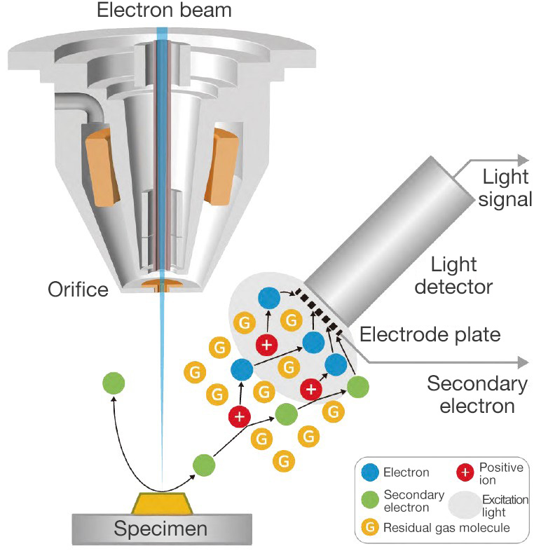
Fig. 1 Principle of LHSED signal acquisition
Table 1 LHSED three modes
| Mode | LSED-E | LSED-P | PD |
|---|---|---|---|
| Vacuum mode | Low vacuum | Low vacuum | Low / High vacuum |
| Electrode plate | Application of voltage | Application of voltage | Without application of voltage |
| Signal | Secondary electron | Light (Excitation from secondary electron) |
Light (Direct excitation from a specimen) |
| Information | Topographic information | Mainly topographic information (light emission information included, slightly though) | Light emission information |
| Details | Acquire secondary electrons generated by the collision of electrons emitted from the specimen with gas molecules | Acquire light generated by collisions between secondary electrons from the sample and gas molecules | Acquire light directly excited from a specimen by irradiation of primary electron beams |
Live image quality of low vacuum secondary electron greatly improved
Acquiring excitation light has improved live image quality, making ease of operation better.
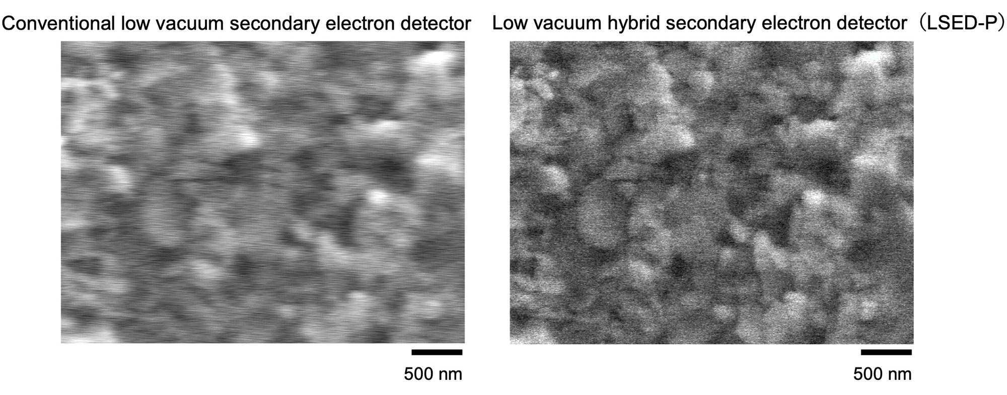
Fig. 2 Low vacuum secondary electron image of business card. Accelerating voltage 5 kV, magnification x 30,000, scan time 0.15 seconds
Acquisition of light emission information by LHSED (PD mode)
When a specimen is irradiated by electron beams, various signals are generated. Electrons in a solid are excited by electron-beam irradiation leaving holes. The electrons recombine with the holes to emit light, which is called "Cathodoluminescence". By acquiring the signals, structures of crystal defects and others in materials can be examined, which can be applied to the analysis of semiconductors and minerals.
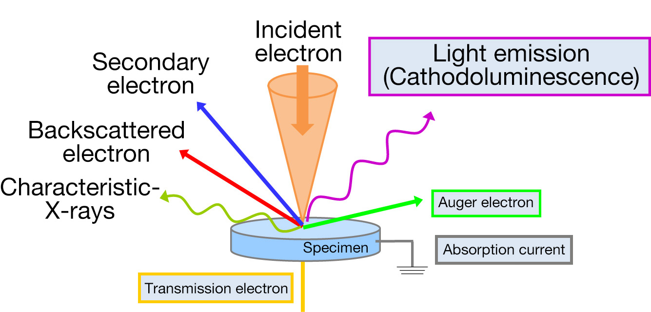
Fig. 3 Various signals generating during electron beam irradiation
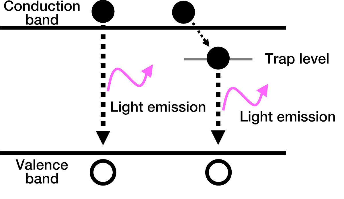
Fig 4 Schematic diagram of CL light emissionCL is generated as extra energy when an electron excited in conduction band or an electron in trap level recombines with a hole in valence band.
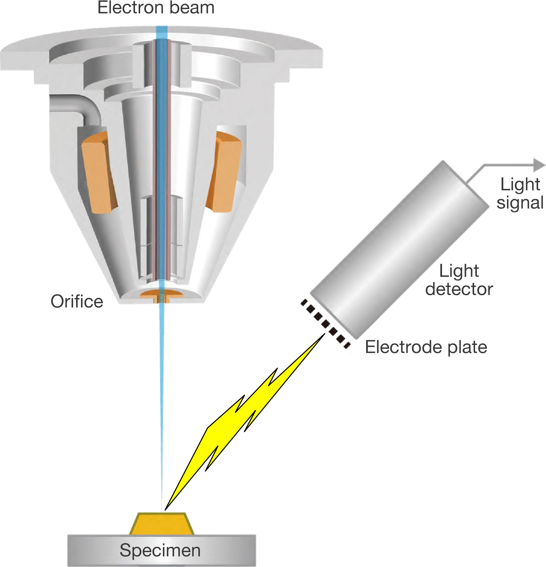
Fig.5 Schematic diagram of signal acquisition in PD mode
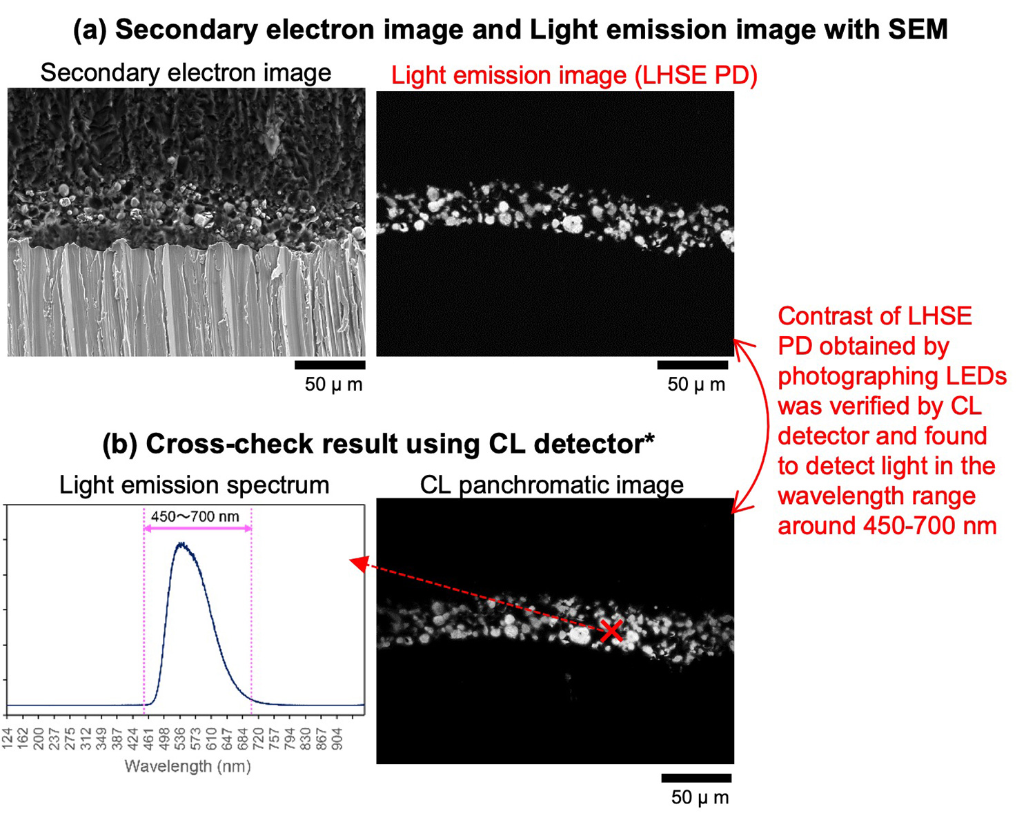
Comparison of light emission information from LED fracture surface between LHSED and CL detector
*CL detector used : CL detector F-CLUE by Horiba Ltd.
Application example using LHSE PD mode
ZnO particle in Zn particle
There are oxides that emit light by electron beam irradiation. Judging an oxide normally requires elemental mapping. However, acquiring a PD image can identify the location of oxides in a short time.
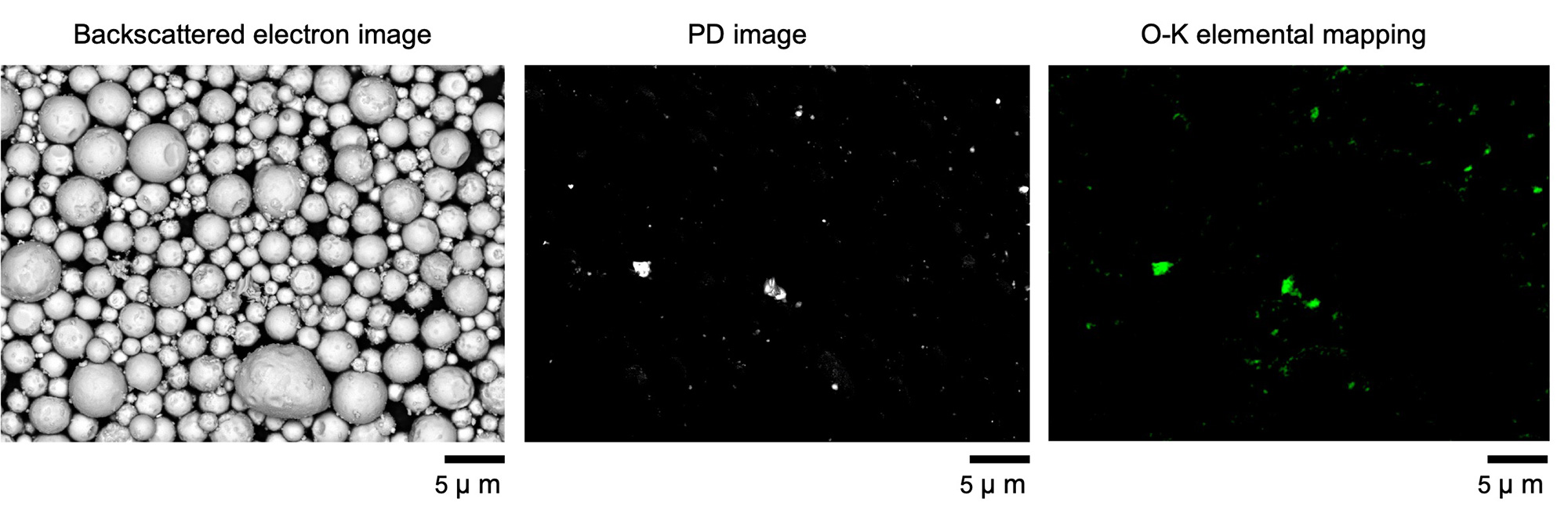
Fig. 7 SEM image and elemental mapping image of Zn particle and ZnO particle in the Zn particles Accelerating voltage : 10 kV, Magnification: x3,000
By combining with the montage function, the distribution of oxides in a wide area can be understood, which is useful for prompt understanding of foreign material distribution.
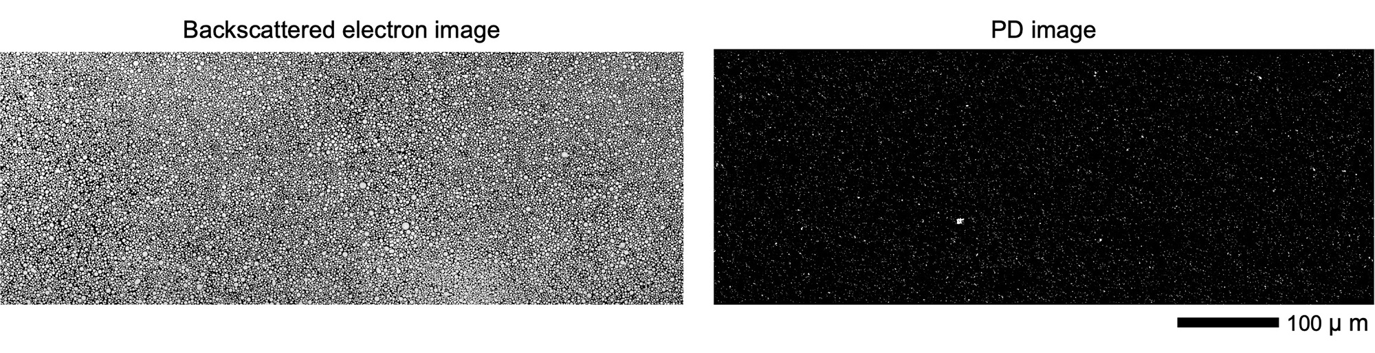
Fig. 8 Montage image of Zn particle and ZnO particle. Accelerating voltage 5 kV, Magnification of 1 field of view x 30,000, Observation range 0.852 x 0.314 mm
Observation of crystal growth striation and crystal defect of minerals
Zircon (ZrSiO4)
Zircon exhibits contrasts derived from defects and impurities that occur during crystal growth. They serve as "tree rings" of the crystal and are useful for analyzing the growth stages.
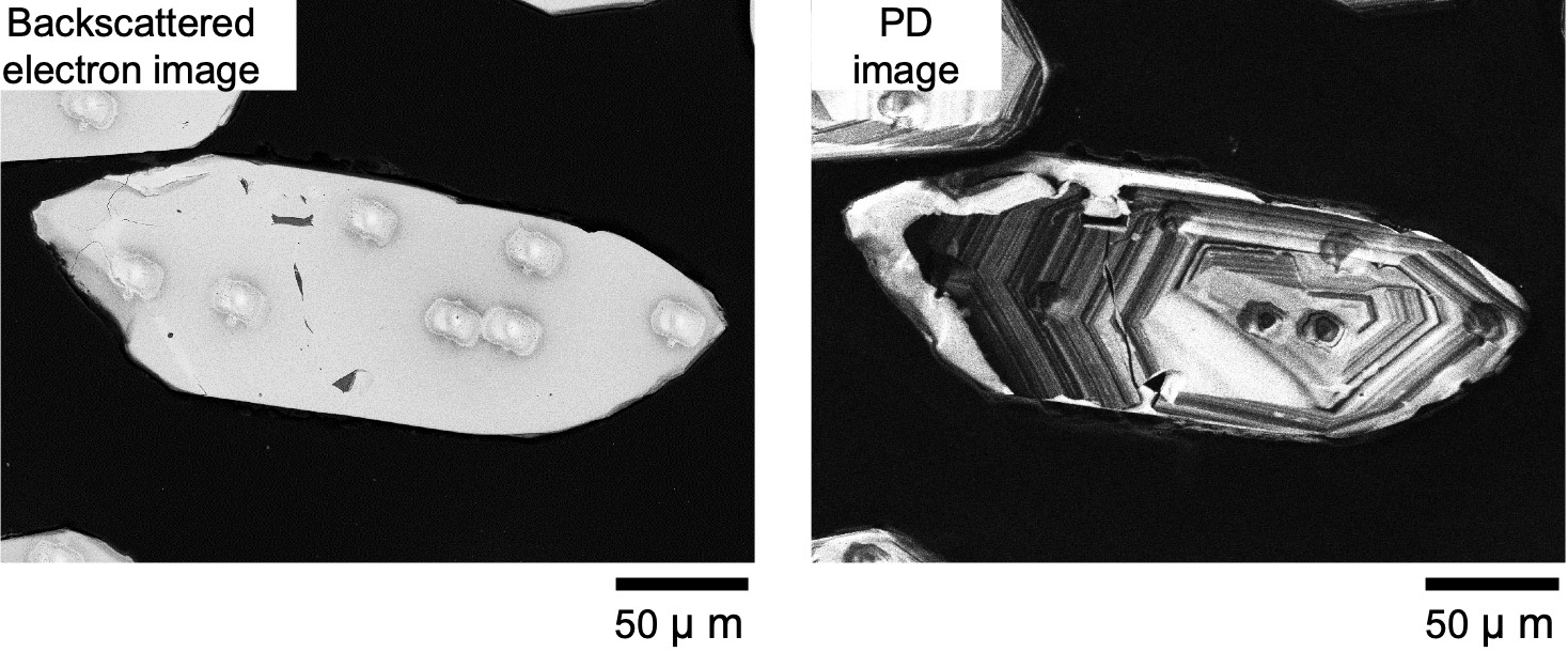
Fig. 9 SEM image of zircon. Accelerating voltage 10kV, Magnification x400
Diamond
Information derived from defects and impurities that occur during crystal growth can be obtained.
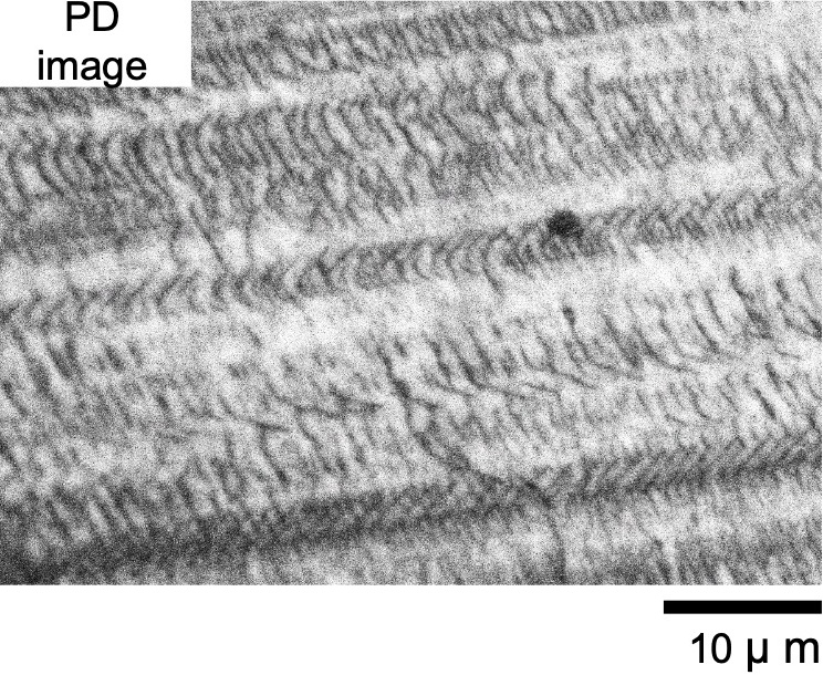
Fig.10 PD image of diamond
Accelerating voltage 5 kV, Magnification x2,500
Dislocation observation of gallium nitride substrate
Gallium nitride (GaN) substrates which are used as power semiconductors, are an inevitable material in life today. As dislocations in the substrate can directly lead to failure of the device, the test to control them is extremely important.
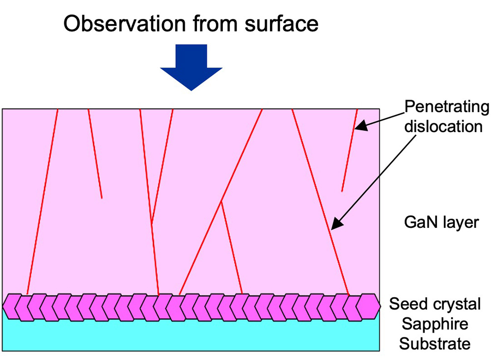
Fig. 11 Cross-sectional schematic diagram of GaN substrate
What is dislocation?
When a slip occurs inside a crystal, the boundary of the slip is called a dislocation(line). The crystal surrounding a dislocation is highly distorted, which also affects the electrical properties of semiconductors and the corrosion resistance of metals.
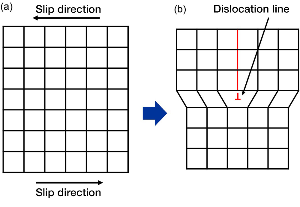
Fig.12 (a) Slip deformation in crystal (b) Dislocation
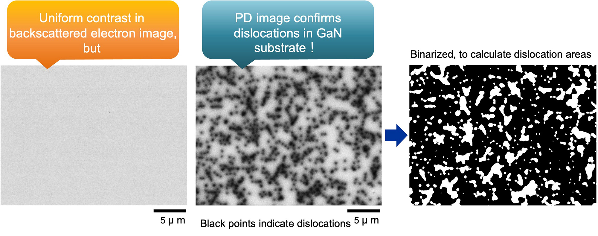
Dislocation area: 491.52 μm2
Percentage of dislocation against the field of view: 30.83%
Combination of PD image and image analysis software can be applied
for testing of dislocation area and dislocation density in GaN.
Summary
The newly developed low-vacuum hybrid secondary electron detector (LHSED) acquires excitation light during residual gas ionization, greatly improving the live image quality of low-vacuum secondary electrons and providing better ease of use. In addition, the LHSED can acquire not only secondary electron images but also light emission images by switching the signal and can qualitatively capture light emission information instantaneously. This allows the LHSED to be used as a partial substitute for a dedicated CL detector.
Solutions by field
Electrical / Electronic Component
Related products
Are you a medical professional or personnel engaged in medical care?
No
Please be reminded that these pages are not intended to provide the general public with information about the products.