The integration of laser and SEM technologies enables high-quality, large-area cross-sectioning and measurements
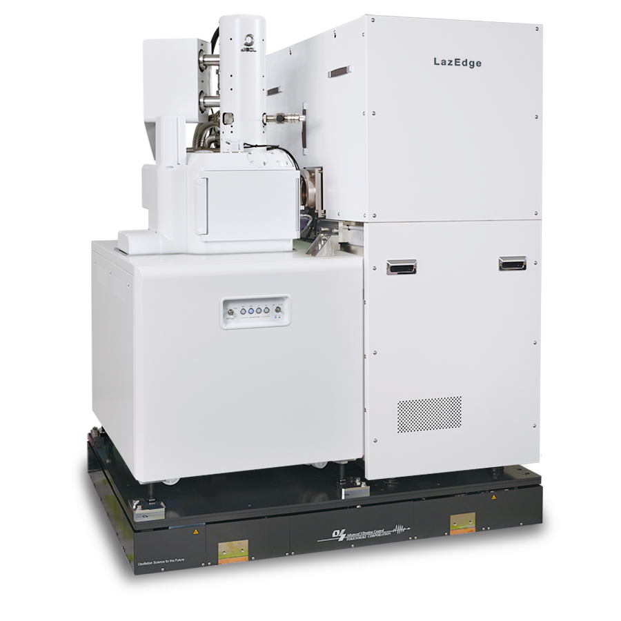
“LazEdge” is an instrument integrating JEOL’s SEM with the laser technology proprietary of Hamamatsu Photonics K.K., and enables laser processing inside the specimen chamber of the electron microscope.
This system enables high-quality cross-section specimens produced through high-speed, large-area processing to be transferred seamlessly to subsequent analyses, such as SEM observation, elemental analysis, and crystal orientation analysis, without exposure to the external environment. As a result, it meets a wide range of analytical needs, including metal specimen analysis, battery analysis requiring air-isolation, and semiconductor failure analysis requiring high-speed cross-sectioning.
Features
An SEM with a Femtosecond Laser Capable of High-Quality Cross-Sectioning is Born
Point. 1
High-quality cross-sectioning in the specimen chamber
By integrating a laser processing system into the SEM, LazEdge delivers high speed, large area cross sectioning within the specimen chamber.
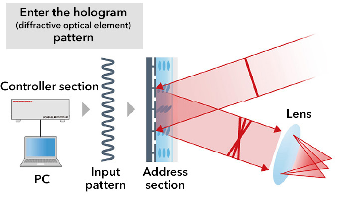
Through the use of a proprietary optical system that enables phase modulation of the laser beam spatially, high quality cross sectioning with reduced LIPSS structures can be achieved.
Point. 2
Contamination prevention in the specimen chamber
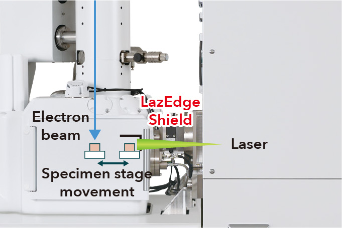
The proprietary shielding technology, LazEdge Shield, prevents debris generated during processing from scattering.
Detectors, columns, specimen chamber walls can be kept clean without contamination.
Point. 3
Seamless operation between laser cross-sectioning⇔SEM observation
Rapid switching between processing and observation is possible within the SEM specimen chamber. Laser processing alone can provide cross-sections of EBSD quality, and 3D EBSD can be achieved by automatically repeating the processing and measurement steps.
Quick processing & measuring of large area due to an integrated laser and SEM
Measurement example of a metal specimen using a wide-area and high-speed processing.
It covers a wide area in a short processing time. From large-area processing to EBSD mapping, the entire process is completed in about one hour. It seamlessly handles operations from processing to analysis at an astonishing speed.
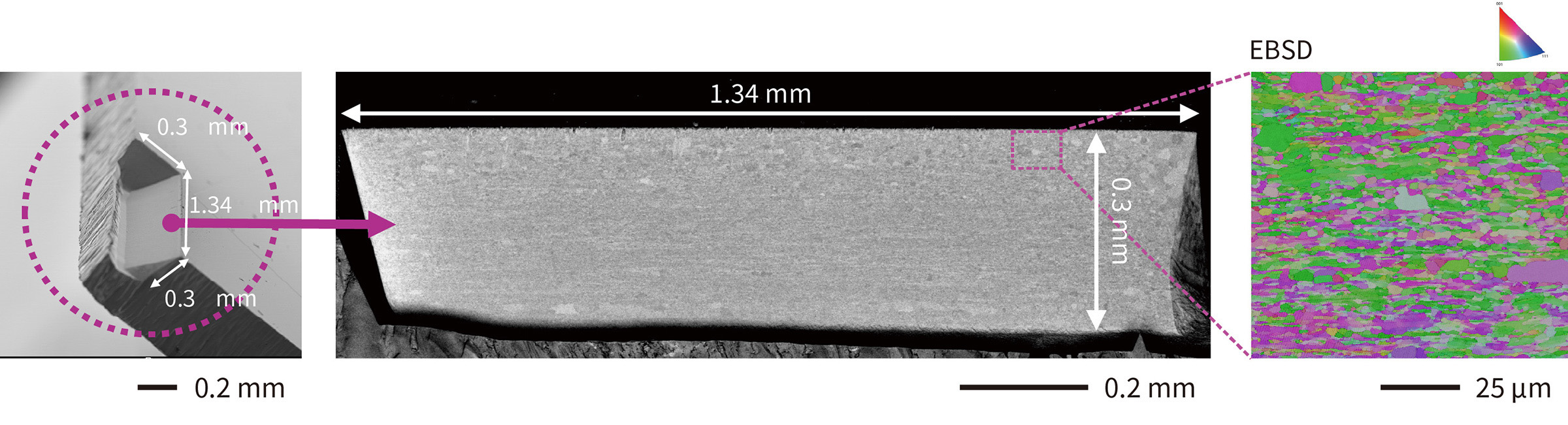
Specimen: Mo plate
Processing time: Approx. 30 minutes
Catalogue Download
Related Products
Scanning Electron Microscope (SEM)
More Info
Are you a medical professional or personnel engaged in medical care?
No
Please be reminded that these pages are not intended to provide the general public with information about the products.