


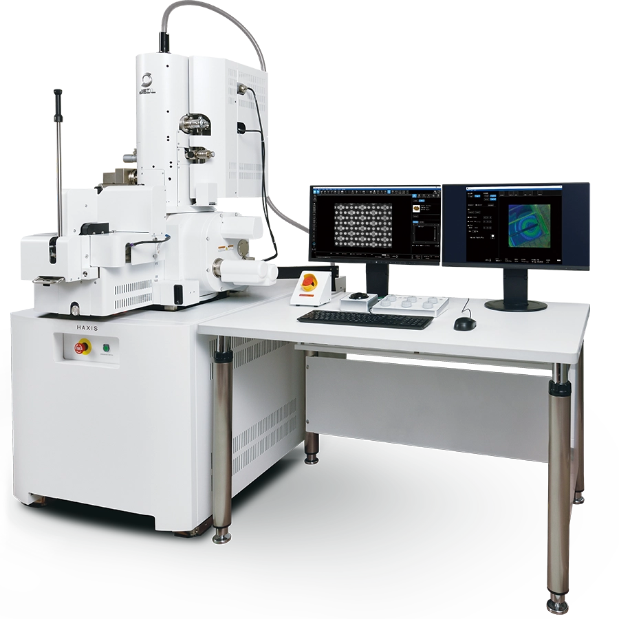
HAXIS
LIM (Low-angle Ion Milling) - SEM
Multi Beam System
PVC-Based Failure Analysis for Advanced Semiconductor Devices
As advanced semiconductor devices continue to shrink with increasing structure complexity, it has become increasingly difficult to directly probe nanoscale circuits using nano-manipulators. In addition, contact caused by probing may affect the analysis target, necessitating new failure analysis methods.
With extensive research on the Passive Voltage Contrast (PVC) detection technology, JEOL has established a new method for stable, highly reproducible PVC observation through the advancement of detector technology and sample preparation techniques.
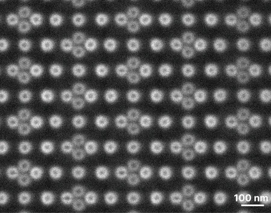
3 nm processing technology
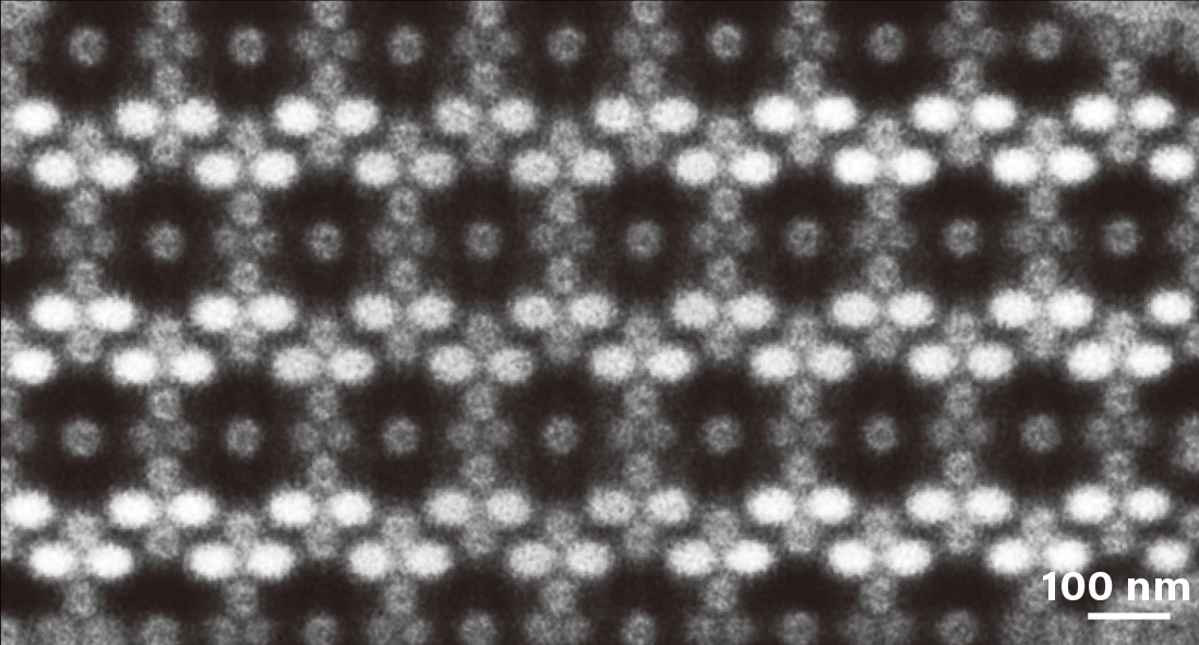
Sample: SRAM (3 nm processing technology) / Landing voltage: 0.3 kV / Detector: UID
LIM-SEM is JEOL’s new semiconductor failure analysis platform that integrates these technologies. It enables clear, highly reproducible PVC imaging, even in advanced semiconductor devices. By visually detecting electrical anomalies while minimizing the effects of processing damage and contamination, LIM-SEM can efficiently locate defects and determine their root cause. The use of the inert gas argon (Ar), ensures stable surface quality while reducing the instrument operation cost.
Approach to Semiconductor Failure Analysis
Rapid Failure Localization and High-Precision Analysis
Semiconductor failure analysis involves multiple steps, from failure localization to physical analysis and root-cause investigation. As device complexity increases, shortening the turnaround time from failure detection to actionable results becomes increasingly critical. LIM-SEM introduces a new approach to failure localization by integrating LIM delayering with SEM imaging and PVC analysis. This combined workflow enables rapid and highly accurate identification of failure locations, supporting QTAT (Quick Turn Around Time) failure analysis and accelerating the transition from electrical failure detection to physical analysis and root-cause identification.
Workflow of Semiconductor Failure Analysis and Diagram of LIM-SEM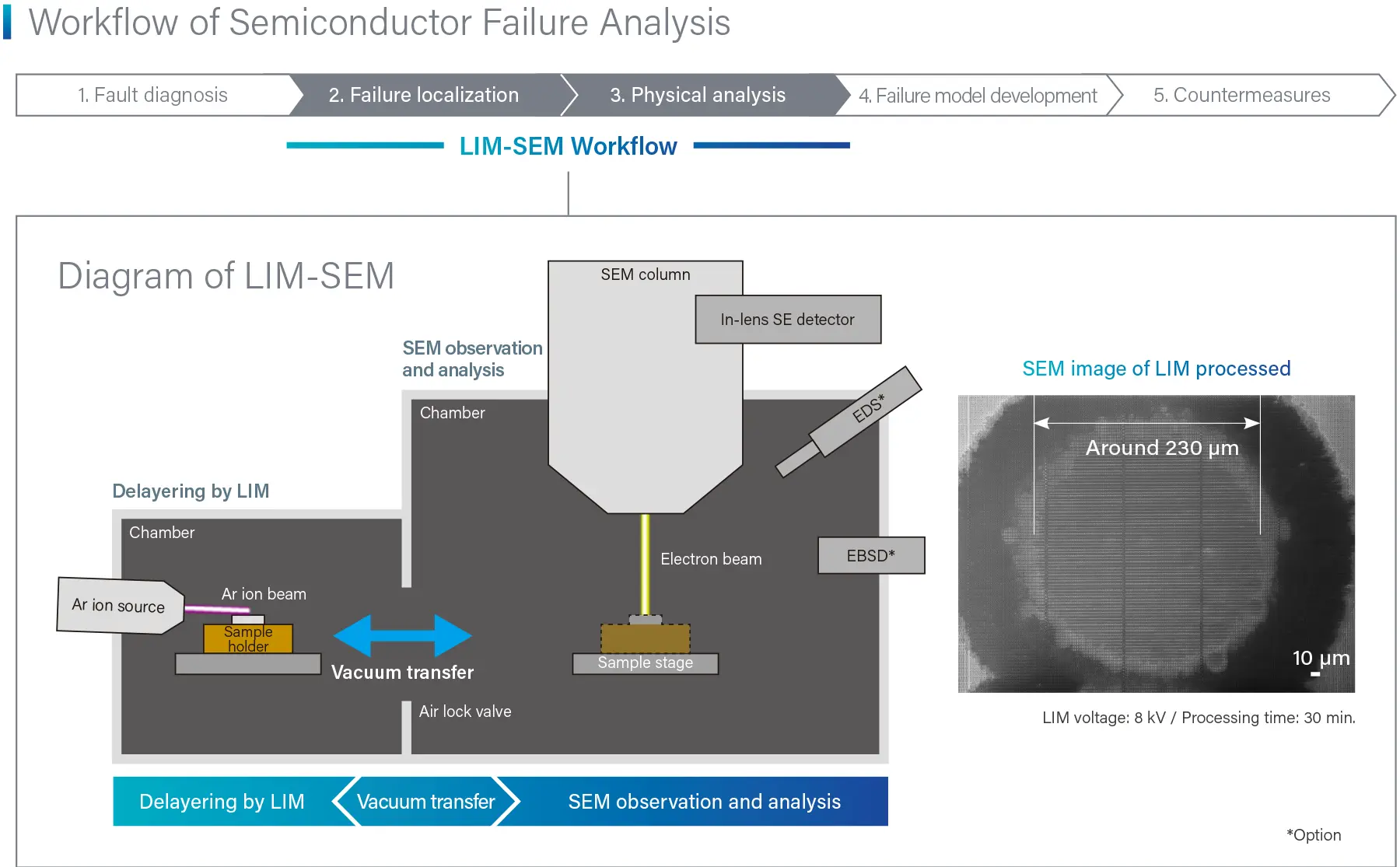
Features
1. Low-Damage LIM Processing for Reliable PVC Observation
The quality of PVC observation is significantly affected by the surface condition of the sample after delayering. LIM-SEM uses a unique Low-angle Ion Milling (LIM) delayering technique using Ar ion beams to create a region of interest (ROI) flat surface with minimal damage. This enables clear and highly reproducible PVC observation while retaining structural and potential information even in advanced devices.

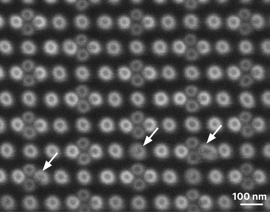
Distortion and contamination caused
by mechanical polishing (arrows)

Flat surface prepared by LIM
Sample: SRAM (7 nm processing technology) / Landing voltage:0.5 kV / Detector: UID
2. Layer-by-Layer LIM/PVC Analysis
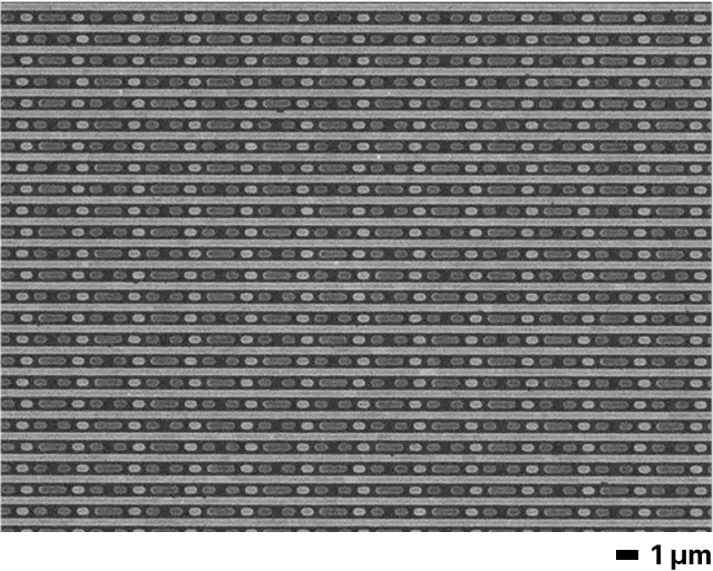
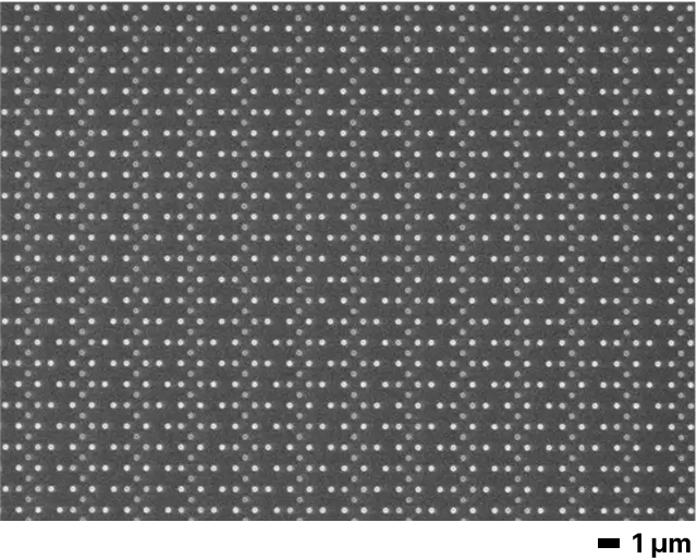
In order to identify the failure location, it is essential to identify the analysis target layer by repeating LIM and PVC observation. LIM-SEM reduces analysis time and improves work efficiency by eliminating the need for moving sample between instruments. By performing analysis in the depth direction while repeating processing and observation, defects within the ROI can be efficiently identified.
Cross section
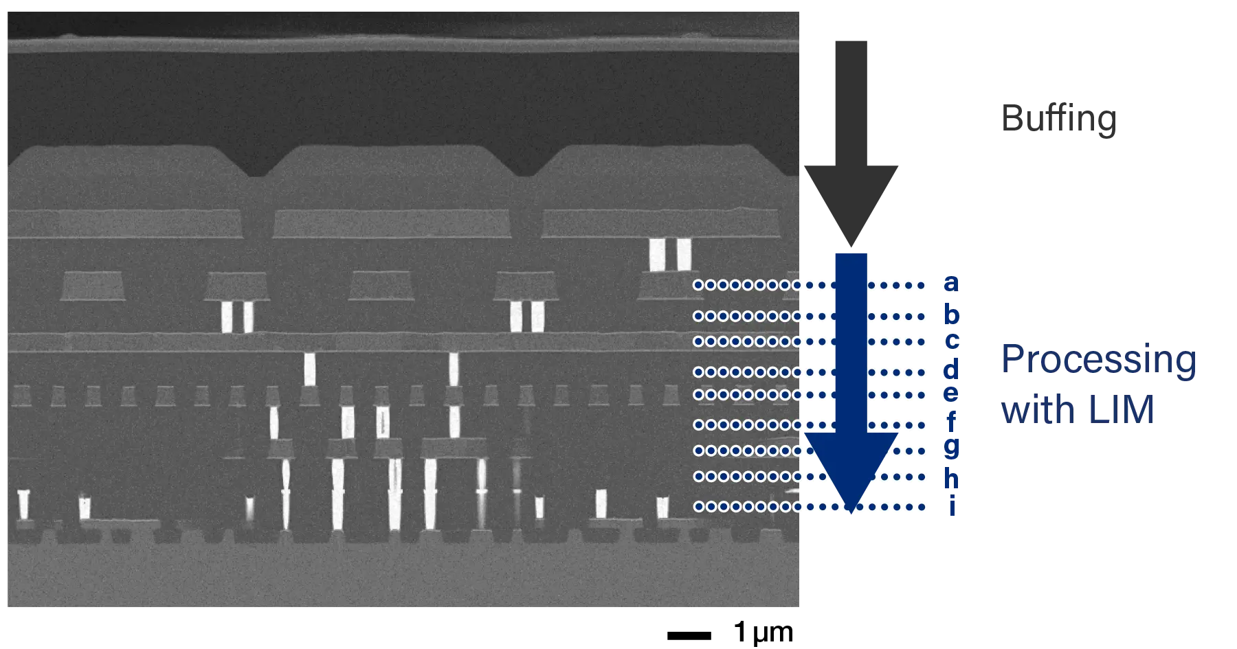
Layer-by-Layer LIM/PVC Analysis by LIM-SEM
a. 2min
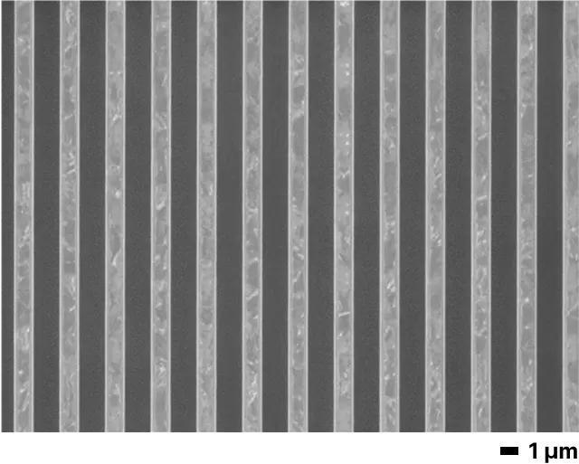
b. 3.5min
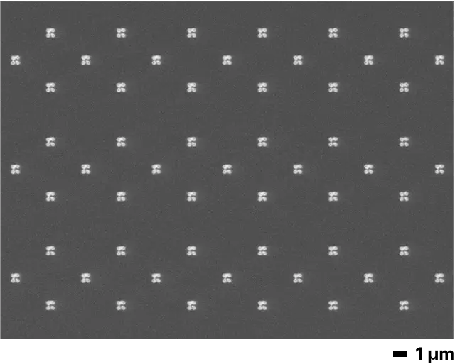
c. 6min
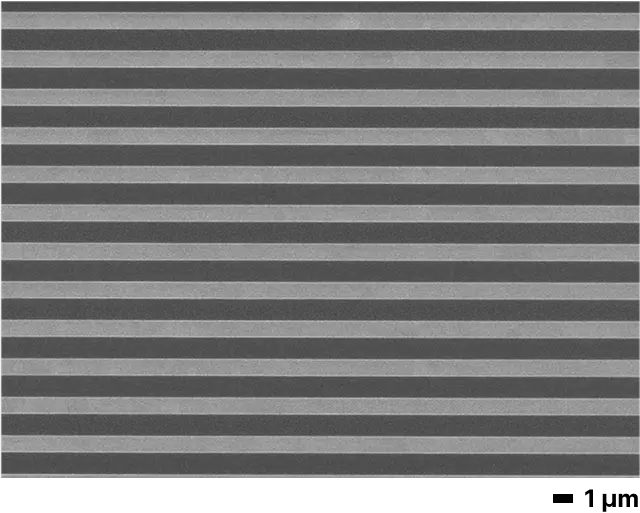
d. 8min
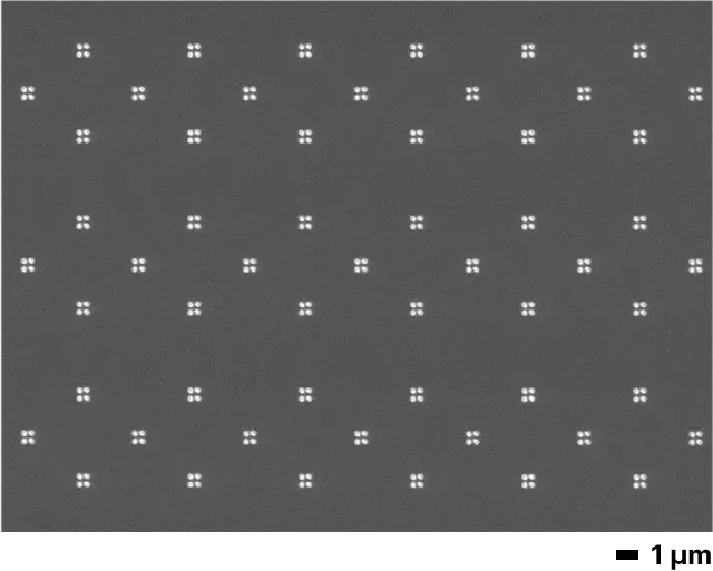
e. 10.5min
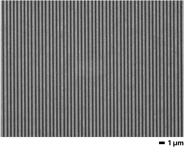
f. 12.5min
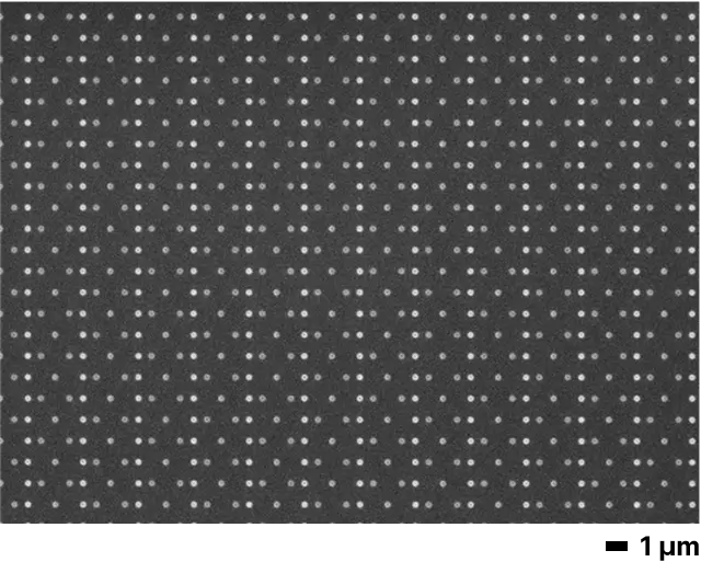
g. 15min
h. 17.5min
i. 20min
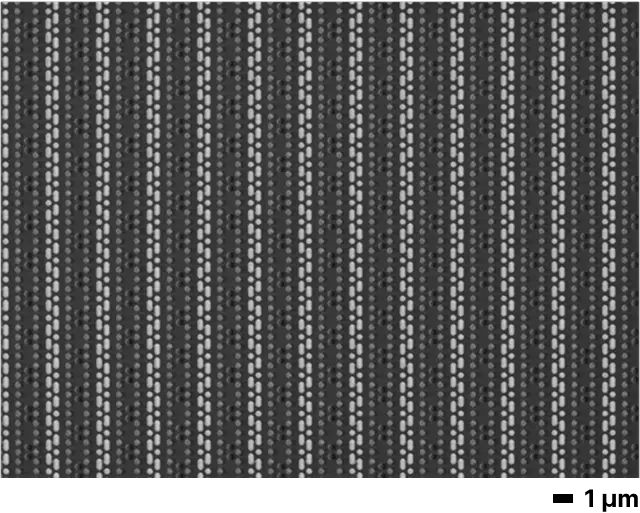
Sample: SRAM / Landing voltage: 0.5 kV / Detector: UID / LIM voltage: 6 kV
3. Vacuum Transfer for Contamination-Free Observation
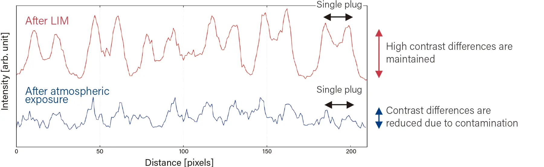
During PVC observation of advanced devices, even slight contamination of the sample surface can significantly impact image quality. Vacuum transfer reduces contamination associated with pretreatment and atmospheric exposure and reduces variability in PVC observation. By keeping the sample surface clean, stable PVC images can be obtained in high magnification observation.
After atmospheric exposure
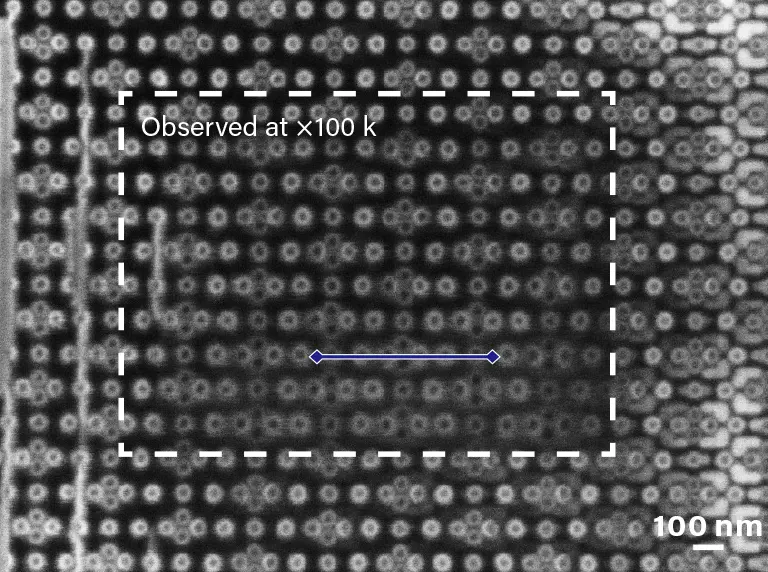
After LIM
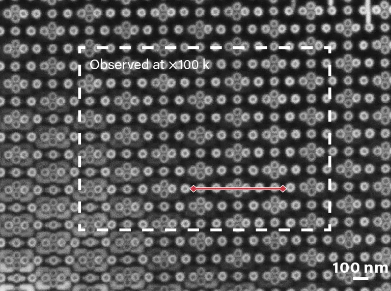
Sample: SRAM (7 nm processing technology) / Landing voltage: 0.5 kV / Detector: UID
4. Enhanced PVC Contrast with VC Filter
As advanced semiconductor devices continue to shrink, it is necessary to clearly visualize the slight potential difference caused by defects. PVC observation uses Secondary Electron (SE) signals, but many of them contain extremely low energy secondary electrons that contribute little to PVC, which can degrade the clarity of the image. By removing these unwanted signals using the Vivid Contrast (VC) filter, the detector can capture clearer PVC changes caused by defects.
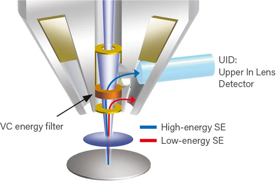
Structure of the VC filter
- Negative voltage applied to the electrode between -50 and 0 V.
→ SE below the applied voltage are rejected - Controllable in 0.1 V steps
→ Optimal conditions according to the sample can be set
VC Filter OFF
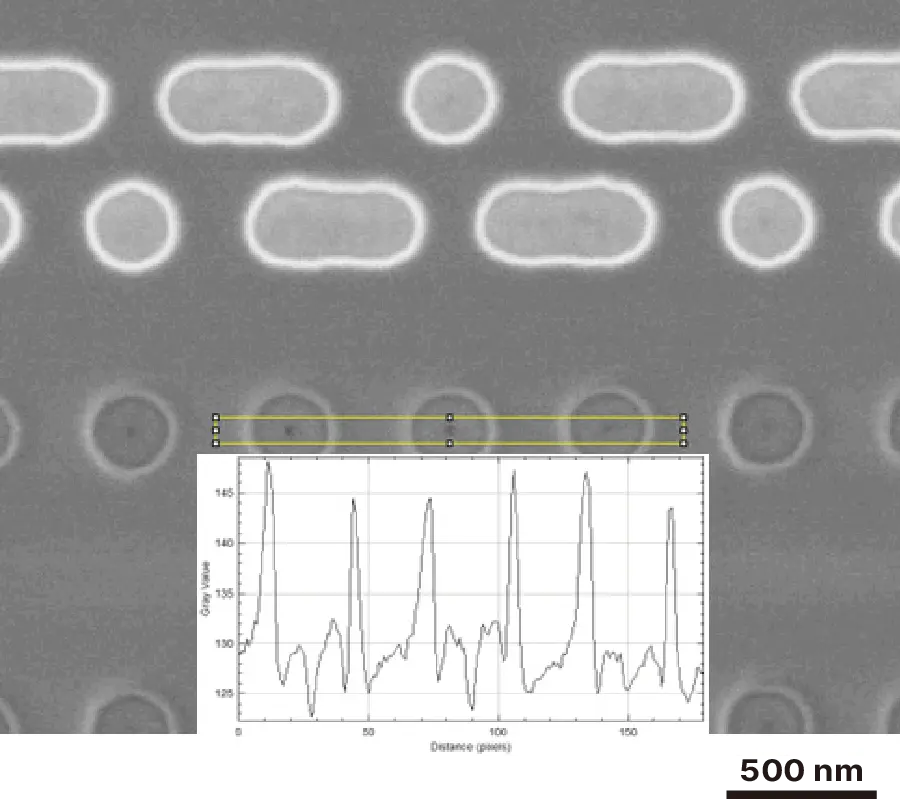
VC Filter ON
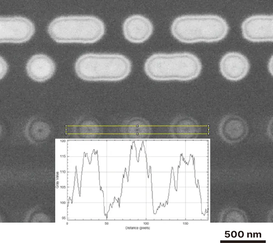
Sample: SRAM / Landing voltage: 1 kV / Detector: UID
Specifications
| Milling range | Diameter of 2,500 μm or more※1 |
|---|---|
| Ion acceleration voltage | 2 to 10 kV (Ion energy 2 to 10 keV) |
| Process Gas | Argon gas |
| Applicable models |
SEM main unit: JSM-IT810 <SIL>※2、<SHL>、<HL> |
※1 Milling conditions: accelerating voltage: 8 kV, sample: Si wafer with oxide film, rotation speed: 3 rpm, milling time: 2 min.
※2 VC Filter available
Catalogue Download
Application
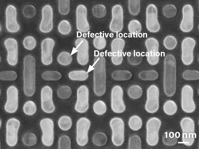
SRAM Failure Observation
If a failure is present in the sample, changes in the PVC can be observed. The PVC reflects minute differences in resistance; plugs with lower resistance appear brighter, while those with higher resistance appear darker. In the sample after LIM, the failure location can be clearly observed.
Defective product
Normal product
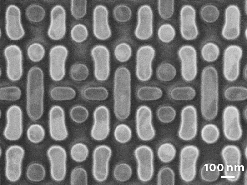
Sample: SRAM / Landing voltage: 1 kV / Detector: UID
3D NAND
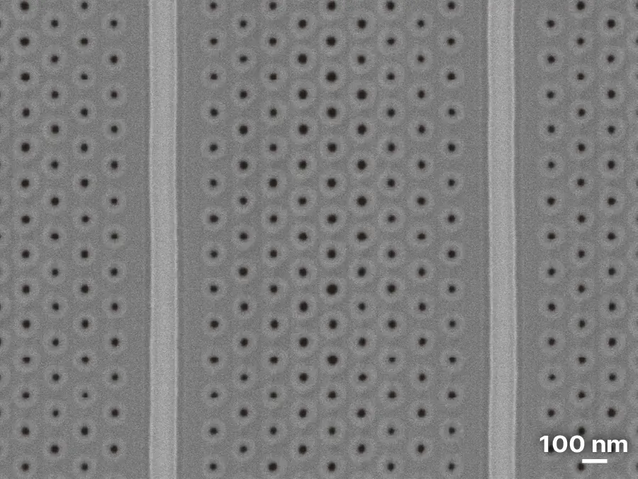
3D NAND has a complex three-dimensional structure consisting of hundreds of alternating metal and insulating layers. The sample was delayered by LIM and the structure of metal and insulating layers was clearly observed in the cell array region.
Insulating layers
Metal layers
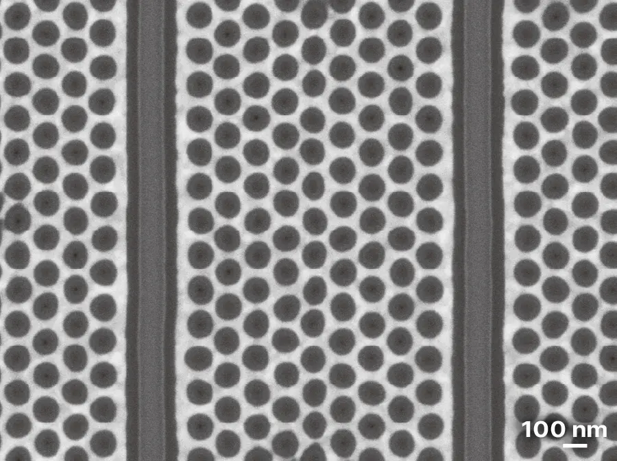
Sample: 3D NAND / Landing voltage: 1 kV / Detector: UID / LIM voltage: 6 kV / Processing time: 39 min.
High-Resolution EBSD Analysis ※Option
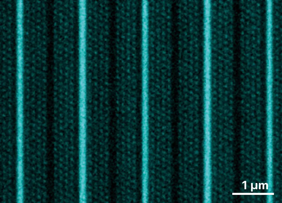
LIM-SEM supports SEM-EDS structural observation and elemental analysis as well as high-resolution EBSD analysis. Thanks to the high-quality machined surface formed by LIM, it is possible to obtain crystal orientation information with high spatial resolution even from 3D NAND high aspect ratio tungsten wiring. This enables evaluation by combining structural information and crystal orientation information.
EDS Analysis W-M
EBSD Analysis
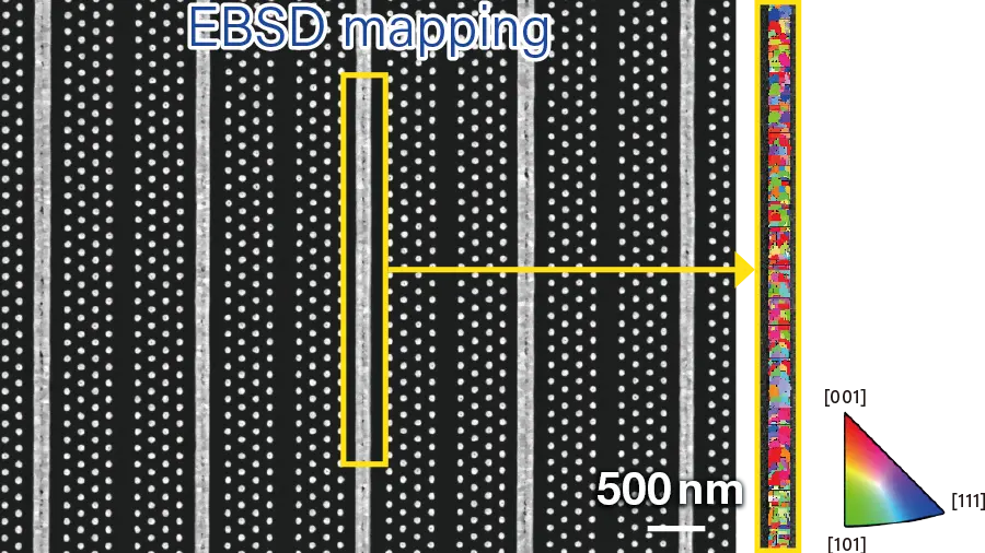
Backscattered electron image observation
Sample: 3D NAND / Landing voltage: 5 kV / Detector: SBED
EBSD Landing voltage: 20 kV / Step mapping: 10 nm
EBSD AZtecHKL SymmetryS3 manufactured by Oxford Instruments
Related Products
More Info
Solutions by field
Semiconductor


Are you a medical professional or personnel engaged in medical care?
No
Please be reminded that these pages are not intended to provide the general public with information about the products.