JEOL-Nikon CLEM Solution Center
Facilities
JEOL Ltd. (President Gon-emon Kurihara) is pleased to announce the “JEOL-Nikon CLEM Solution Center”, a collaborative project between Nikon and JEOL Ltd., was established on September 1, 2017. The center will be opened in the R & D Building of JEOL to provide experience in and collect and deliver technical information on cutting-edge CLEM* solutions.
* CLEM: Correlative Light & Electron Microscopy
Overview of the JEOL-Nikon CLEM Solution Center
| Address | JEOL Ltd., 3-1-2 Musashino, Akishima, Tokyo |
|---|---|
| Major installations | Optical microscopes (stereo microscopes, industrial microscopes, confocal laser microscope systems)
electron microscopes (transmission electron microscopes, scanning electron microscopes, electron probe microanalyzers), and various types of sample preparation equipment |
| Tel | +81-3-6262-3567 |
| Demonstration | Please contact the Center to arrange a demonstration. Demonstrations are by appointment only. |
CLEM is an effective observation and analysis method that combines the advantages of two microscope types: optical microscopes, which allow fast wide field observation and acquisition of the positional and localization information of molecules, and electron microscopes, which allow acquisition of minute structure data by observation of samples under high spatial resolution. In recent years, the need for more effectively using CLEM, by linking optical and electron microscopes via software, has increased in cutting-edge bioscience and material development research.
In 2013, JEOL developed the “miXcroscopy™ Linked Optical & Scanning Electron Microscopy System” in collaboration with Nikon. Furthermore, in February 2014, JEOL signed a capital and business alliance agreement with Nikon, and has promoted cooperation between the two companies to build CLEM solution that combine Nikon’s optical microscopes and JEOL’s electron microscopes, as well as enhancing product development and sales capabilities.
At the new Solution Center, we will introduce “miXcroscopy™”, and offer CLEM solutions to promote the use of CLEM. We will also collect and deliver information that will improve CLEM technology through dialogue with our customers, and contribute to generating new benefits in bioscience and material development research.
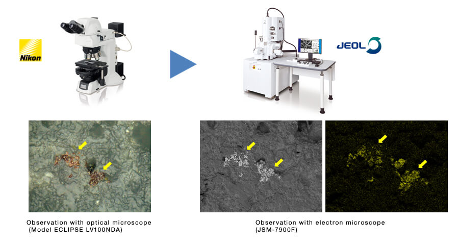
Example: CLEM observation of foreign materials on glass ceramics
Detecting foreign substances using an optical microscope (left), capturing those high resolution image using an electron microscope (center), and analyzing their composition through characteristic X-ray analysis using an electron microscope (right). As a result, the foreign substance is identified as iron. CLEM enables fast and precise detection, identification and analysis of foreign substances, and more efficient inspection and analysis of product quality, contributing to the improvement of productivity in factories and laboratories.